SK Hynix Mulls 'Differentiated' HBM Memory Amid AI Frenzy
by Anton Shilov on March 1, 2024 3:30 PM EST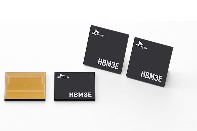
SK Hynix and AMD were at the forefront of the memory industry with the first generation of high bandwidth memory (HBM) back in 2013 – 2015, and SK Hynix is still leading this market in terms of share. In a bid to maintain and grow its position, SK Hynix has to adapt to the requirements of its customers, particularly in the AI space, and to do so it's mulling over how to make 'differentiated' HBM products for large customers.
"Developing customer-specific AI memory requires a new approach as the flexibility and scalability of the technology becomes critical," said Hoyoung Son, the head of Advanced Package Development at SK Hynix in the status of a vice president
When it comes to performance, HBM memory with a 1024-bit interface has been evolving fairly fast: it started with a data transfer rate of 1 GT/s in 2014 – 2015 and reached upwards of 9.2 GT/s – 10 GT/s with the recently introduced HBM3E memory devices. With HBM4, the memory is set to transit to a 2048-bit interface, which will ensure steady bandwidth improvement over HBM3E.
But there are customers which may benefit from differentiated (or semi-custom) HBM-based solutions, according to the vice president.
"For implementing diverse AI, the characteristics of AI memory also need to become more varied," Hoyoung Son said in an interview with BusinessKorea. "Our goal is to have a variety of advanced packaging technologies capable of responding to these changes. We plan to provide differentiated solutions that can meet any customer needs."
With a 2048-bit interface, many (if not the vast majority) of HBM4 solutions will likely be custom or at least semi-custom based on what we know from official and unofficial information about the upcoming standard. Some customers might want to keep using interposers (but this time they are going to get very expensive) and others will prefer to install HBM4 modules directly on logic dies using direct bonding techniques, which are also expensive.
Making differentiated HBM offerings requires sophisticated packaging techniques, including (but certainly not limited to) SK Hynix's Advanced Mass Reflow Molded Underfill (MR-RUF) technology. Given the company's vast experience with HBM, it may well come up with something else, especially for differentiated offerings.
"For different types of AI to be realized, the characteristics of AI memory also need to be more diverse," the VP said. "Our goal is to have a range of advanced packaging technologies to respond to the shifting technological landscape. Looking ahead, we plan to provide differentiated solutions to meet all customer needs."
Sources: BusinessKorea, SK Hynix


10 Comments
View All Comments
ballsystemlord - Friday, March 1, 2024 - link
Not to complain about AT, but that press release is completely devoid of information."To service AI workloads, HBM-something is going to be manufactured sometime for someone somewhere."
Is all that really need to be printed in this article.
nandnandnand - Friday, March 1, 2024 - link
How about HBM for consumer products hahahhhahhoohhooheheheheBZD - Sunday, March 3, 2024 - link
Worked well with the Rage Fury.ballsystemlord - Sunday, March 3, 2024 - link
It's the HBCC, not so much the HBM, that really made Vega a good card.boozed - Sunday, March 3, 2024 - link
High Bandwidth Memory Memorynandnandnand - Monday, March 4, 2024 - link
AnandTech really didn't like the discussion about how it's dying. Sad!Ryan Smith - Tuesday, March 5, 2024 - link
It's a discussion better suited for our forums, than at the top of a news post.PeachNCream - Thursday, March 7, 2024 - link
It is their site and if they don't want comments discussing its decline in readership and content quality, they have every right to hide it by deleting comments about it to control damage.Kevin G - Wednesday, March 6, 2024 - link
I wonder for custom solutions if more exotic implementations are possible. For example independent read write buses to remove turn-around time latencies. Another radical idea would be implement custom HBM as SRAM using a leading edge node (<5 nm). Despite a single SRAM needing multiple transistors, these are about to eclipse the densities used by DRAM and their single bit capacitor mechanism. The different process nodes for DRAM have not kept up with logic.bananaforscale - Wednesday, March 13, 2024 - link
There's apparently something about SRAM that doesn't shrink well with node improvements.