SK Hynix Shows Off 321-Layer 3D TLC NAND Device
by Anton Shilov on August 9, 2023 8:30 AM EST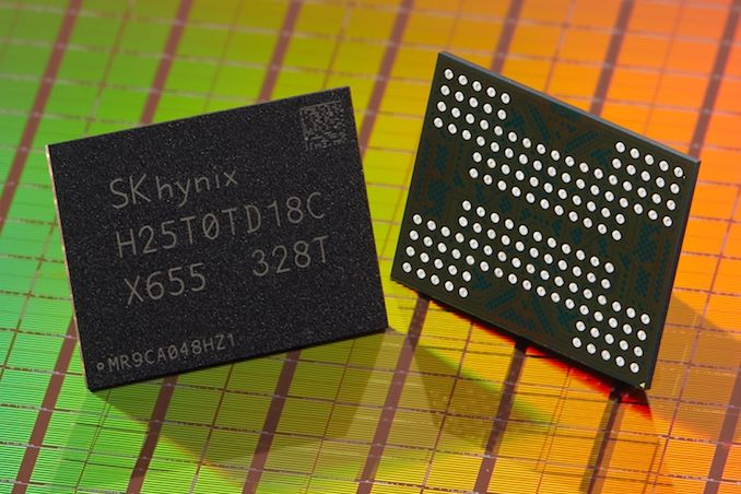
SK Hynix showcased its 321-layer TLC NAND memory at the Flash Memory Summit 2023. The South Korean company is the first NAND maker to publicly demonstrate 3D NAND with over 300 layers. Although such memory is expected in mass production in 2025, the demonstration is meant to showcase SK Hynix's preparedness for the next wave of non-volatile memory technology.
This showcased 321-layer 3D NAND memory device boasts a 1 Tb (128 GB) capacity with TLC architecture, but SK Hynix refrained from revealing other details about it, such as interface speed. Meanwhile, the company mentioned that the chip features a 59% improvement in productivity compared to a 512 Gb 238-layer 3D TLC device, highlighting a significant improvement in per-wafer storage density. Whether or not the new production technology significantly reduces the cost-per-bit of 3D NAND is unclear.
SK Hynix using a 1 Tb 3D TLC device to demonstrate the prowess of its 321-layer 3D NAND process technology may be a good sign, and the company intends to build high-capacity 3D devices on this node. The potential means reduced cost-per-bit compared to existing process nodes. This sets the stage for higher-capacity SSDs and other 3D NAND flash-bases storage devices.
While SK Hynix has yet to reveal the specifics of building 321 active layers, it is safe to assume that the manufacturer used string stacking technology, just like the industry uses it for 200+ layer 3D NAND. However, it is unclear whether SK Hynix stacked two ~160-layer stacks on top of each other or managed to put three ~100+ stacks together.
SK Hynix's 321-layer 3D TLC NAND device continues to use the company's CMOS-under-array architecture that puts NAND logic below memory cells to save die space, which is why SK Hynix refers to it as 4D NAND, which is essentially a marketing term.
"With another breakthrough to address stacking limitations, SK Hynix will open the era of NAND with more than 300 layers and lead the market," said Jungdal Choi, head of NAND development at SK Hynix, during a keynote speech. "With timely introduction of the high-performance and high-capacity NAND, we will strive to meet the requirements of the AI era and continue to lead innovation."
Source: SK Hynix


9 Comments
View All Comments
GC2:CS - Wednesday, August 9, 2023 - link
If we really give up the nice and tidy power of 2 layers, does that mean we will also give up the capacities ? And each product will have some random capacity determined by number of layers ?Sounds confusing, decadic system is too complicated to me.
Kristian Vättö - Wednesday, August 9, 2023 - link
It's a 1Tbit (128GB) die. The number of layers simply refers to the number of active memory layers and it's still possible to build dies in capacities of power of 2.Lonyo - Wednesday, August 9, 2023 - link
If it's 321, then one might assume it would be 3x10⁷ layersabufrejoval - Wednesday, August 9, 2023 - link
3-2-1, can't help but thinking that it sounds a bit ominous for a storage device...PeachNCream - Wednesday, August 9, 2023 - link
It's great for rocket launches though - unless said rocket has a SpaceX logo on it which would imply detonation on or just above the launch pad and a billowing cloud in the shape of a certain Twitter owner's face.Jansen - Friday, August 11, 2023 - link
Guess you’ve never heard of a Falcon 9.PeachNCream - Friday, August 11, 2023 - link
Yes, I have heard of that branding for SpaceX explosions.meacupla - Wednesday, August 9, 2023 - link
why? Endurance of >1TB SSD using 3D nand is extremely good.Diogene7 - Sunday, August 13, 2023 - link
I wish it would be possible to do the same with Non-Volatile Memory (NVM) MRAM : 1Tb (128GB) (VCMA) MRAM die, non volatile, fast and low power memory would open so maly new opportunities in mobile and Internet of Things (IoT) devices