SK hynix Intros LPDDR5T Memory: Low Power RAM at up to 9.6Gbps
by Ryan Smith on January 25, 2023 10:30 AM EST
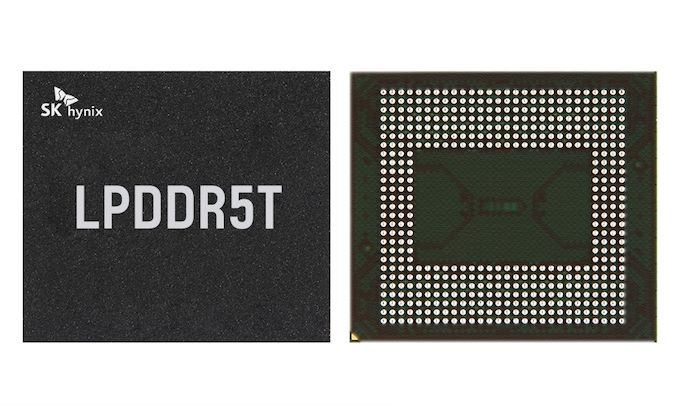
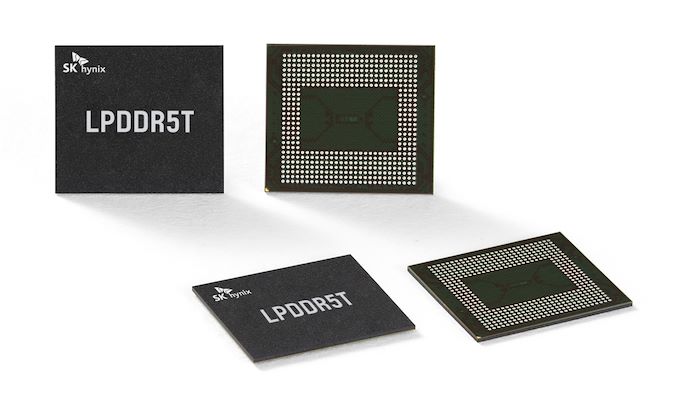
In a bit of a surprise move, SK hynix this week has announced a new variation of LPDDR5 memory technology, which they are calling LPDDR5T. Low Power Double Data Rate 5 Turbo (LPDDR5T) further ramps up the clockspeeds for LPDDR5-type memory, with SK hynix stating that their new memory will be able to clock at high as 9.6Gbps/pin, 13% faster than their top-bin 8.5Gbps LPDDR5X. According to the company, the memory is sampling now to partners as a 16GB part, with mass production set to begin in the second half of this year.
SK hynix is positioning LPDDR5T as an interim memory technology to cover the gap between LPDDR5X and the future development of LPDDR6, offering what amounts to a half-step up in memory bandwidth for customers who would like something faster than what contemporary LPDDR5X memory is capable of. That standard, as it currently stands, only goes to 8533Mbps, so any LPDDR5-type memory clocked higher than that is technically outside of the official JEDEC specification. Still, SK hynix’s announcement comes a bit unexpectedly, as while it’s not unusual for memory manufacturers to announce new technologies ahead of the industry’s standardization body, there hadn’t been any previous chatter of anyone coming to market with a further evolution of LPDDR5.
At this point the technical details on the new memory are limited. SK hynix was able to confirm that LPDDR5T will operate at the same voltages as LPDDR5X, with a VDD voltage range of 1.01v to 1.12v (nominally 1.05v) and a VDDQ of 0.5v. Coupled with that, as previously mentioned the new memory will max out at a data rate of 9.6Gbps/pin, which for a 64-bit part would mean a full data rate of 76.8GB/second. Otherwise, at this point all outward appearances are that LPDDR5T is just higher clocked LPDDR5X, given a new name since its data rate is outside the scope of LPDDR5X.
| LPDDR Generations | ||||||
| LPDDR4 | LPDDR4X | LPDDR5 | LPDDR5X | LPDDR5T (Provisional) |
||
| Max Density | 64 Gbit | 32 Gbit | 32 Gbit? | |||
| Max Data Rate | 4266Mbps | 6400Mbps | 8533Mbps | 9600Mbps | ||
| Channels | 2 | 1 | 4? | |||
| Width | x32 (2x x16) | x16 | x64 | |||
| Banks (Per Channel) |
8 | 8-16 | 16? | |||
| Bank Grouping | No | Yes | Yes? | |||
| Prefetch | 16n | 16n | 16n? | |||
| Voltage | 1.1v | Variable Nominal: 1.05v Max: 1.1v |
Variable Nominal: 1.05v Max: 1.12v |
|||
| Vddq | 1.1v | 0.6v | 0.5v | |||
But whatever LPDDR5T is (or isn’t), SK hynix tells us that they intend to make a proper JEDEC standard of it. The company is already working with JEDEC on standardization of the memory technology, and while this doesn’t guarantee that other memory vendors will pick up the spec, it’s a sign that LPDDR5T isn’t going to be some niche memory technology that only ends up in a few products. This also means that the rest of the pertinent technical details should be published in the none too distant future.
In the meantime, for their initial LPDDR5T parts, SK hynix is going to be shipping a multi-die chip in a x64 configuration. According to the company’s PR office, they’re producing both 12Gb and 16Gb dies, so there’s a potential range of options for package densities, with the 16GB (128Gbit) package being the largest configuration. All of this RAM, in turn, is being built on the company’s 1anm process, which is their fourth-generation 10nm process using EUV, and paired with High-K metal gates (HKMG).
SK hynix’s decision to go with only a x64 package out of the gate is a notable one, since these higher density packages are typically limited to use in high-end smartphones and other high-performance devices (laptops, servers, etc), underscoring the intended market. For their part, SK hynix has stated that they expect the application of LPDDR5T to “expand beyond smartphones to artificial intelligence (AI), machine learning and augmented/virtual reality (AR/VR)”. LPDDR memory has been seeing increasing use in non-mobile products, so this doesn’t come as a surprise given the high-end nature of the technology. Server hardware vendors in particular come to mind as potential customers, since those products can easily absorb any increased power consumption from the higher memory clockspeeds.
Wrapping things up, SK hynix says that they expect to begin mass production of LPDDR5T in the second half of this year. So depending on just when in the year that production begins, and when their downstream customers implement the new RAM, it could begin showing up in products as easy as the end of this year.
Source: SK hynix


10 Comments
View All Comments
nandnandnand - Wednesday, January 25, 2023 - link
https://hothardware.com/news/innosilicon-lpddr5x-d...Here's a demo of LPDDR5X-10000. This 'T' name is marketing BS.
lmcd - Wednesday, January 25, 2023 - link
The official product name cannot use X designation. The standard is named and done, and unlike consumer RAM, overclocking is not an option.nandnandnand - Wednesday, January 25, 2023 - link
JEDEC has published two updates to the DDR5 spec. I'm sure they can do the same with LPDDR5X and raise the maximum allowed speeds.meacupla - Wednesday, January 25, 2023 - link
does it really work at 9600Mbps, or is it 4800Mbps x2?because if it's the latter, isn't that just quad channel?
Ryan Smith - Wednesday, January 25, 2023 - link
9600Mbps would be the per pin rate. Memory speeds are measured per pin, not per package.meacupla - Wednesday, January 25, 2023 - link
Okay, in that case, this stuff looks like a win for soldered on RAM.brucethemoose - Wednesday, January 25, 2023 - link
So that's 384 bits for the equivalent bandwidth of the RTX 4070 TI's 192-bit, 504GB/s bus.A 1024-bit bus like the dual-die M1 Max would be 1.2TB/s, higher than 1TB/s on the 4090 (but still less than an A100).
I hope some wide, low power stuff comes out of this.
schujj07 - Thursday, January 26, 2023 - link
This will be used in laptops and phones where you usually have 128bit and 64bit buses.brucethemoose - Thursday, January 26, 2023 - link
Yeah thats what I figured, but some exotic, wide designs (like the M1/M2 Max) would be cool.mode_13h - Wednesday, March 15, 2023 - link
Nvidia's Grace is using in-package LPDDR5X, similar to Apple's M-series. The main difference is that Grace is a server-oriented CPU, and Nvidia was willing to forego memory upgradability mainly for the power-savings of putting it in-package. Current configuration is 480 GB per CPU.https://developer.nvidia.com/blog/nvidia-grace-cpu...