The Snapdragon 888 vs The Exynos 2100: Cortex-X1 & 5nm - Who Does It Better?
by Andrei Frumusanu on February 8, 2021 3:00 AM EST- Posted in
- Mobile
- Samsung
- Qualcomm
- Smartphones
- SoCs
- Snapdragon 888
- Exynos 2100
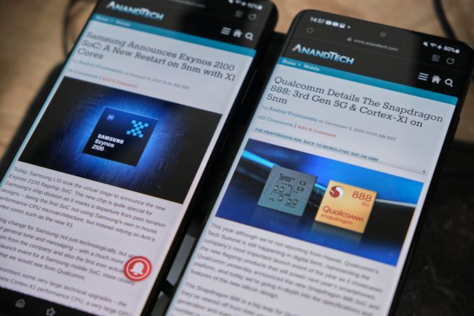
The new Galaxy S21 series of devices have been out commercially for a week now, and we’ve managed to get our hands on two Galaxy S21 Ultras – one with Qualcomm’s new Snapdragon 888 SoC, and one with Samsung’s new Exynos 2100 SoC. Both chipsets this year are more similar than ever, both now sporting similar CPU configurations, and both being produced on a new Samsung 5nm (5LPE) process node.
Ahead of our full device review of the Galaxy S21 Ultra (and the smaller Galaxy S21), today we’re focusing on the first test results of the new generation of SoCs, putting them through their paces, and pitting them against each other in the new 2021 competitive landscape.
The Snapdragon 888
| Qualcomm Snapdragon Flagship SoCs 2020-2021 | |||
| SoC | Snapdragon 865 |
Snapdragon 888 |
|
| CPU | 1x Cortex-A77 @ 2.84GHz 1x512KB pL2 3x Cortex-A77 @ 2.42GHz 3x256KB pL2 4x Cortex-A55 @ 1.80GHz 4x128KB pL2 4MB sL3 |
1x Cortex-X1 @ 2.84GHz 1x1024KB pL2 3x Cortex-A78 @ 2.42GHz 3x512KB pL2 4x Cortex-A55 @ 1.80GHz 4x128KB pL2 4MB sL3 |
|
| GPU | Adreno 650 @ 587 MHz | Adreno 660 @ 840MHz | |
| DSP / NPU | Hexagon 698 15 TOPS AI (Total CPU+GPU+HVX+Tensor) |
Hexagon 780 26 TOPS AI (Total CPU+GPU+HVX+Tensor) |
|
| Memory Controller |
4x 16-bit CH @ 2133MHz LPDDR4X / 33.4GB/s or @ 2750MHz LPDDR5 / 44.0GB/s 3MB system level cache |
4x 16-bit CH @ 3200MHz LPDDR5 / 51.2GB/s 3MB system level cache |
|
| ISP/Camera | Dual 14-bit Spectra 480 ISP 1x 200MP or 64MP with ZSL or 2x 25MP with ZSL 4K video & 64MP burst capture |
Triple 14-bit Spectra 580 ISP 1x 200MP or 84MP with ZSL or 64+25MP with ZSL or 3x 28MP with ZSL 4K video & 64MP burst capture |
|
| Encode/ Decode |
8K30 / 4K120 10-bit H.265 Dolby Vision, HDR10+, HDR10, HLG 720p960 infinite recording |
8K30 / 4K120 10-bit H.265 Dolby Vision, HDR10+, HDR10, HLG 720p960 infinite recording |
|
| Integrated Modem | none (Paired with external X55 only) (LTE Category 24/22) DL = 2500 Mbps 7x20MHz CA, 1024-QAM UL = 316 Mbps 3x20MHz CA, 256-QAM (5G NR Sub-6 + mmWave) DL = 7000 Mbps UL = 3000 Mbps |
X60 integrated (LTE Category 24/22) DL = 2500 Mbps 7x20MHz CA, 1024-QAM UL = 316 Mbps 3x20MHz CA, 256-QAM (5G NR Sub-6 + mmWave) DL = 7500 Mbps UL = 3000 Mbps |
|
| Mfc. Process | TSMC 7nm (N7P) |
Samsung 5nm (5LPE) |
|
Starting off with the new Snapdragon 888 SoC, Qualcomm’s new flagship model makes iterative steps this generation, with the biggest changes of the new design actually being in the form of the new Hexagon 780 accelerator, which fuses together traditional scalar and vector DSP operations with tensor execution engines within one single IP block.
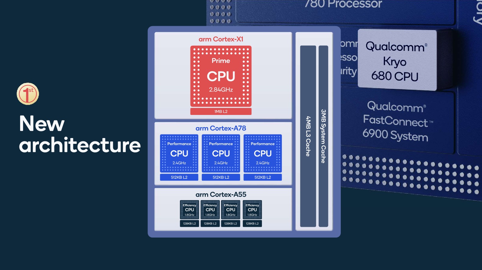
Of course, we’re also seeing upgrades elsewhere in the architecture, with the Snapdragon 888 being among the first SoCs to use Arm’s new Cortex-X1 CPU IP, promising large performance gains relative to last generation Cortex-A77 cores. The single X1 cores in the Snapdragon 888 clocks in at 2.84GHz – the same as the previous generation Snapdragon 865’s prime Cortex-A77 cores, and less than the 3.1GHz and 3.2GHz Snapdragon 865+ and recently announced Snapdragon 870 SoCs.
Alongside the X1, we find three Cortex-A78 cores at 2.42GHz, again the same clocks as the previous generation 865 SoCs, but this time around with double the L2 caches at 512KB.
The Cortex-A55 little cores remain identical this generation, clocking in at 1.8GHz.
Although we had been expecting 8MB L3 cache flagship SoCs this year, it does look like Qualcomm opted to remain at 4MB for this generation – but at least the company dons the X1 core with the maximum 1MB L2 cache configuration.
On the GPU side of things, Qualcomm’s new Adreno 660 GPU now clocks in up to a peak 840MHz – a whopping 43% higher frequency than the Snapdragon 865 GPU. The company’s performance claims here are also astonishing, promising a +35% boost in performance. We’ll have to see how this all ends up in terms of power consumption and long-term performance in the later dedicated GPU section.
What’s quite different for the Snapdragon 888 this year is that Qualcomm has moved from a TSMC N7P process node to Samsung’s new 5LPE node – the generally wildcard in this whole situation as we haven’t had any prior experience with this new 5nm node.
The Exynos 2100
| Samsung Exynos SoCs Specifications | ||
| SoC |
Exynos 990 |
Exynos 2100 |
| CPU | 2x Exynos M5 @ 2.73GHz 2MB sL2 3MB sL3 2x Cortex-A76 @ 2.50GHz 2x256KB pL2 4x Cortex-A55 @ 2.00GHz 4x64KB pL2 1MB sL3 |
1x Cortex-X1 @ 2.91GHz 1x512KB pL2 3x Cortex-A78 @ 2.81GHz 3x512KB pL2 4x Cortex-A55 @ 2.20GHz 4x64KB pL2 4MB sL3 |
| GPU | Mali G77MP11 @ 800 MHz | Mali G78MP14 @ 854 MHz |
| Memory Controller |
4x 16-bit CH @ 2750MHz LPDDR5 / 44.0GB/s 2MB System Cache |
4x 16-bit CH @ 3200MHz LPDDR5 / 51.2GB/s 6MB System Cache |
| ISP | Single: 108MP Dual: 24.8MP+24.8MP |
Single: 200MP Dual: 32MP+32MP (Up to quad simultaneous camera) |
| NPU | Dual NPU + DSP + CPU + GPU 15 TOPs |
Triple NPU + DSP + CPU + GPU 26 TOPs |
| Media | 8K30 & 4K120 encode & decode H.265/HEVC, H.264, VP9 |
8K30 & 4K120 encode & 8K60 decode H.265/HEVC, H.264, VP9 AV1 Decode |
| Modem | Exynos Modem External (LTE Category 24/22) DL = 3000 Mbps 8x20MHz CA, 1024-QAM UL = 422 Mbps ?x20MHz CA, 256-QAM (5G NR Sub-6) DL = 5100 Mbps (5G NR mmWave) DL = 7350 Mbps |
Exynos Modem Integrated (LTE Category 24/18) DL = 3000 Mbps 8x20MHz CA, 1024-QAM UL = 422 Mbps 4x20MHz CA, 256-QAM (5G NR Sub-6) DL = 5100 Mbps UL = 1920Mbps (5G NR mmWave) DL = 7350 Mbps UL = 3670 Mbps |
| Mfc. Process | Samsung 7nm (7LPP) |
Samsung 5nm (5LPE) |
On the Samsung LSI side of things, we find the brand-new Exynos 2100. Unlike the Snapdragon 888’s more incremental changes in terms of SoC design, the new Exynos is a rather large departure for Samsung’s SoC division as this is the first flagship design in many years that no longer uses Samsung’s own in-house CPU microarchitecture, but rather reverts back to using Arm Cortex cores, which in this case is also the new Cortex-X1 and Cortex-A78 cores.
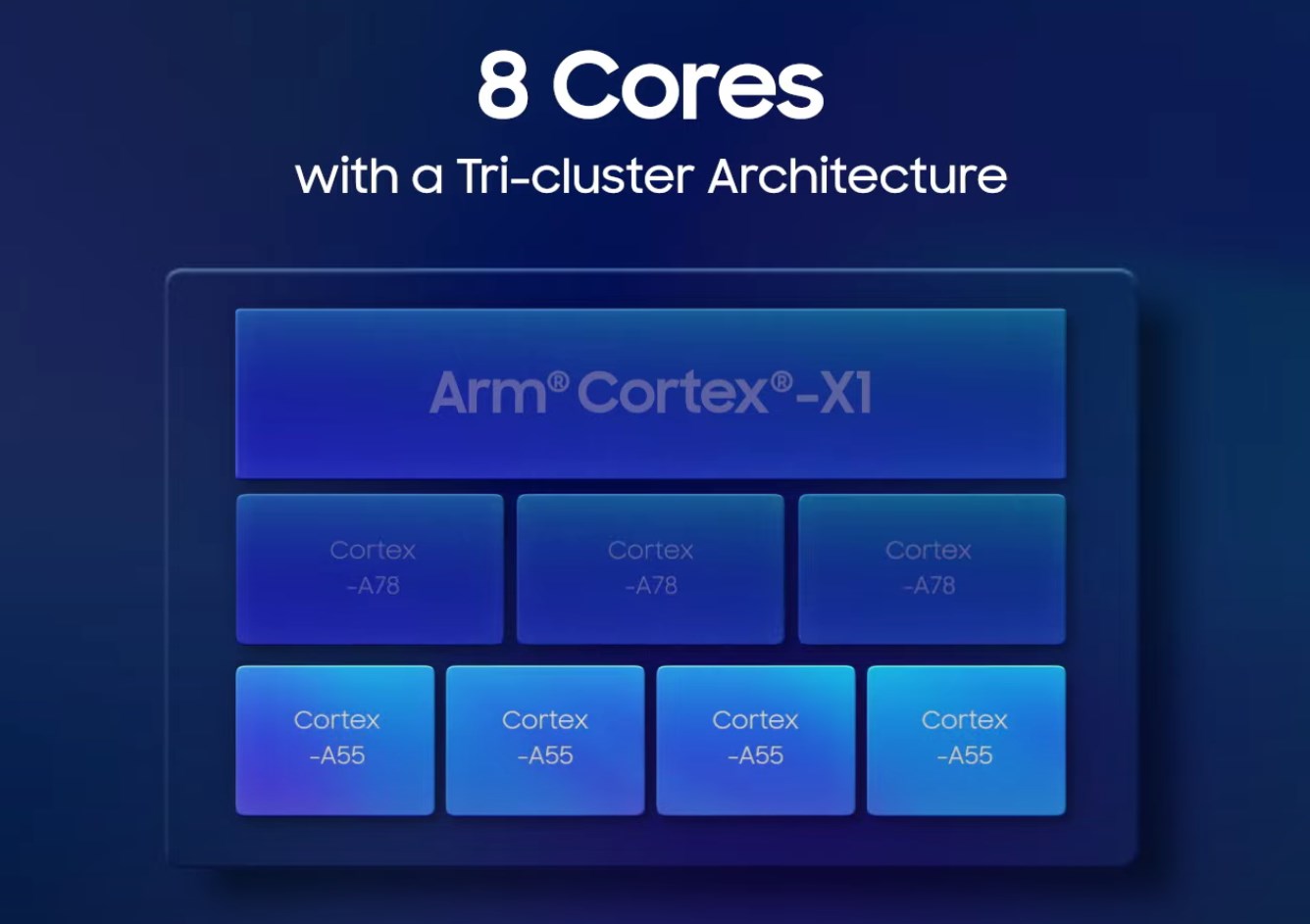
From a high-level, the CPU configuration of the Exynos 2100 looks nigh identical to that of the Snapdragon 888, as both are 1+3+4 designs with X1, A78 and A55 cores. The differences are in the details:
The X1 cores on the Exynos 2100 clock slightly higher at up to 2.91GHz, while the Cortex-A78 clock in significantly higher than the Snapdragon as they reach 2.81GHz. The Cortex-A55 cores are also quite aggressive in terms of frequency as they now reach 2.20GHz – so overall across the board higher clocks than the Snapdragon variant.
Where the Exynos isn’t as aggressive though is in its cache configurations. Most importantly, the X1 cores here only feature 512KB of L2 cache, which is a bit weird given the all-out-performance philosophy of the new CPU. The Cortex-A78s also see the usage of 512KB L2 caches, while the little A55 cores feature 64KB L2’s – less than the Snapdragon counterparts.
Much like the Snapdragon, the L3 cache also falls in at 4MB rather than the 8MB we would have hoped for this generation, however Samsung does surprise us with the usage of an estimated 6-8MB system level cache, up from the 2MB design in the Exynos 990.
On the GPU side of things, we see a Mali-G78MP14 at up to 854MHz. That’s 27% more cores and 6.7% higher frequency, and the company is also boasting massive performance gains as it touts a 40% generational improvement.
Let them fight
In today piece, we’ll be mostly focusing around CPU and GPU performance, as an especially interesting comparison will be to see how the two designs do against each other, given that they both now use Arm’s newest Cortex-X1 cores and both are sporting the same manufacturing node.
The GPU comparisons will also be interesting – and maybe quite controversial, as the results won’t be what many people will have been expecting.
While we would have liked to showcase AI performance of the two SoCs – unfortunately the software situation on the Galaxy S21’s right now means that neither SoC are fully taking advantage of their new accelerators, so that’s a topic to revisit in a few months’ time once the proper frameworks have been updated by Samsung.


123 Comments
View All Comments
serendip - Monday, February 8, 2021 - link
I'm interested in what this means for the SD8cx successor. A 30% increase from using one or two X1 cores would be great, I'm using the SQ2 chip and that's fast enough for typical office tasks. That's still not enough to get within striking range of the M1 or even A14. What the heck is in those Firestorms that makes them so fast?On memory subsystems, what are Qualcomm and Samsung doing wrong compared to Apple and HiSilicon? The M1's memory bandwidth is astonishingly high but that's from using custom parts. HiSilicon is doing a great job using standard ARM interconnects.
Agreed on the stupidly high GPU clocking. The SQ2 has a beefy GPU that performs well but it can get hot even in a large tablet form factor. It's time to stop the marketing departments from forcing engineers to chase pointless metrics.
ikjadoon - Monday, February 8, 2021 - link
>What the heck is in those Firestorms that makes them so fast?A trifecta that I share with people because this question comes up so often.
Technical Part 1: https://www.anandtech.com/show/16226/apple-silicon...
Technical Part 2: https://www.anandtech.com/show/16252/mac-mini-appl...
Consumer + Approachable: https://www.youtube.com/watch?v=3SG5e4z-Ygg
Technical Background + More Approachable: https://www.youtube.com/watch?v=cAjarAgf0nI
As Upscaled wrote, "It's not magic. It's good design." And why don't AMD / Intel have these same good designs? The videos above give thorough answers. For example, the last link explains why everyone cares Firestorm (A14) and Lightning (A13) have an 8-wide decode, which is one of many major "better designs" versus competing Arm & x86 CPUs.
ikjadoon - Monday, February 8, 2021 - link
Uh, wait. Delete. I definitely skipped too much of that one. What on Earth is he going on about 1T vs 1C?~~ Consumer + Approachable: https://www.youtube.com/watch?v=3SG5e4z-Ygg ~~
Wow, I'm a little stunned at how bad this Upscaled video is. The Dev Doc + AnandTech are much more reliable.
Nicon0s - Monday, February 8, 2021 - link
LoL, Engadget.He keeps saying multithreading when he means SMT or Hyperthreading(Intel's version of SMT).
ikjadoon - Monday, February 8, 2021 - link
Yes! Never mind 1T / 1C have shown negligence IPC differences in general computing. 1% at best. Please go test an i5-8600K vs an i7-8700K: one has SMT, one does not. Terrible to see the WCCFTech disinformation cycle reach a mainstream audience so quickly.https://www.anandtech.com/show/16261/investigating...
And then he, out of left field, throws up a Cinebench multi-core score: "See? Intel and Apple are actually very close to each other." But, his comparison was the 4+4 M1 vs an 8C Intel...
I wish I could edit comments. I give up on consumer YouTube videos; I saw his earlier interview with RISC's founders and it seemed halfway decent. I'm a fool.
Archer_Legend - Tuesday, February 9, 2021 - link
Don't be offended but I think that what you posted is completely bs.First of all you are comparing arm64 cpus and x86 cpus, second the arm 64 cores used by apple are very arguably faster than the x86 cores of for example a ryzen cpu.
The second thing which I would want to point out is that about the widht of the pipeline, it is not that apple is a genious or intel and amd are stupid: the x86 architecture was built to have a narrowish pipeline and do more cycles in fact the width of the pipeline in intel and amd cpus is as wide as it gets.
Arm arch on the other end lets you use a wider pipeline, however saying using a narrower or wider pipeline is better or not is pointless because performance comes down to how you organise the cpu around that specific pipeline so....
leledumbo - Monday, February 8, 2021 - link
> What the heck is in those Firestorms that makes them so fast?The same thing since A9 again (CMIIW): super wide decoder + super big cache. Apple isn't stingy when it comes to die size and Apple SoCs are always bigger than Snapdragon on the same generation and process node. 4mm^2 difference is huge when we're talking at nm level. What's weird, Exynos is even bigger but can't match these two. No idea what Samsung put there.
Santoval - Tuesday, February 9, 2021 - link
"What's weird, Exynos is even bigger but can't match these two. No idea what Samsung put there."This is probably due to TSMC having a *far* denser 5nm process node compared to Samsung's process 5nm node. Per the article below TSMC's 5nm node tops at 173 million transistors per mm^2 while Samsung's 5nm node reaches only 126.5 MTr/mm^2 (i.e. barely denser than TSMC's second gen 7nm+ node) due to much more, er, "conservative" design choices (Samsung basically just switched from DDB cells in 7nm to SDB cells; the article explains what that means).
What is often not clear is that the quoted transistor densities of each process node are always the *maximum* transistor densities, not the actual transistor densities used to fab a die. For instance Intel have three different 10nm node variants with three different densities, a low, mid and high density variant (ranging I believe from ~55 million to ~100 million transistors per mm^2). The last one is the only one that has been widely reported, the other two were intended for the tech savvy press and audience.
Each Intel 10nm die has a mix of all three libraries, but each design is (obviously) *fixed* with a precise mix of the three. The desktop parts always have a higher percentage of low density cells because these need to clock higher, and vice versa for the mobile parts. Mobile phones are efficiency focused, so their SoCs have the highest percentage of the highest density variant of each process node that is possible (without hindering performance too much).
That is an additional reason their clocks top at ~3 GHz. Since the two SoCs of the article are both mobile SoCs of an almost identical design we can assume a roughly equivalent percentage of the highest density cells each process node maxes out at. Thus, if all else was being equal (including the same iGPU) Samsung's SoC would have a roughly ~27% larger die than TSMC's SoC. That must be the main reason Samsung kept the cache sizes of the X1 and the A55 cores low.
Santoval - Tuesday, February 9, 2021 - link
p.s. Sorry, I forgot the link to the article :https://semiwiki.com/semiconductor-manufacturers/s...
Santoval - Tuesday, February 9, 2021 - link
p.s.2 I just noticed that the Snapdragon 888 is also fabbed with Samsung's 5nm node. While that rendered the comparison between the two SoCs in my above comment moot the other things I pointed out might have some "academic" value regarding process nodes (I have no away to delete the comment anyway..).