TSMC Updates on Node Availability Beyond Logic: Analog, HV, Sensors, RF
by Dr. Ian Cutress on August 25, 2020 11:00 AM EST
Most of the time when we speak about semiconductor processes, we are focused on the leading edge of what is possible. Almost exclusively that leading edge is designed for logic circuitry where performance and power efficiency are key drivers of pushing the boundaries, but also there’s a strong market in it. Other markets use semiconductor technology where there are other factors to consider: power, analog capabilities, voltage, and memory, all use semiconductor fabs but they are rarely at the leading edge. Nonetheless, the pureplay foundry businesses aims to offer enough technologies and features to cater as needed, along with driving which markets can use which technologies. At TSMC’s Technology Symposium this week, the company gave is a holistic view of its offerings.
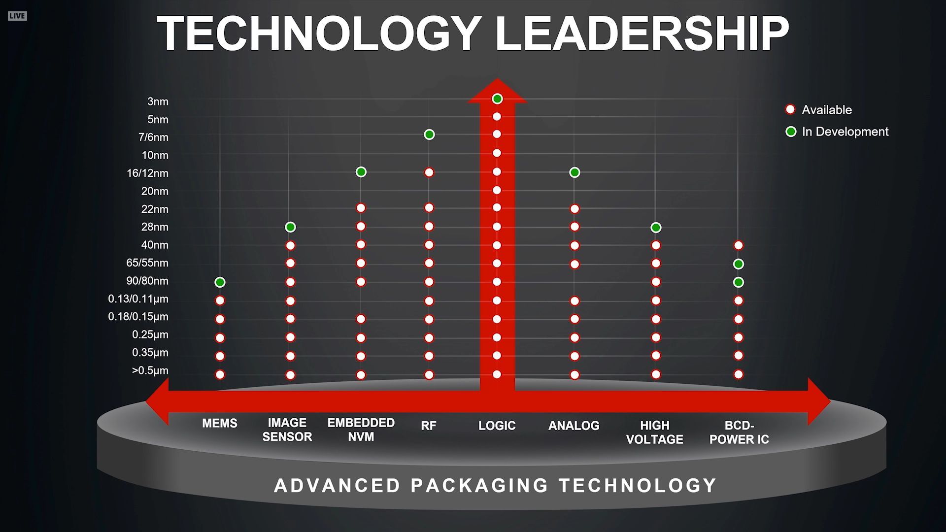
As always, the key central pillar is logic. It also contributes most to revenue, and helps drive the rest of the company, so it’s an important arm of the business. Here TSMC offers all the way up to 5nm, which is currently in high-volume manufacturing ready for the first products by the end of the year. Companies that have 5nm products planned for this year and early next year already have test chips in house built on 5nm. The 3nm node is currently in development.
RF (radio frequency) silicon, used in modems, often sits on the right hand of logic given its importance in the smartphone and mobile connectivity space. Companies have to decide whether to combine logic and RF onto a single monolithic design, or offer logic and RF on separate connected dies. As it stands, TSMC’s RF capabilities have already shown some RF solutions on the leading nodes, but TSMC still very much sees this as a work in progress. At the current time, TSMC is developing its N6 RF technologies for discrete RF solutions.
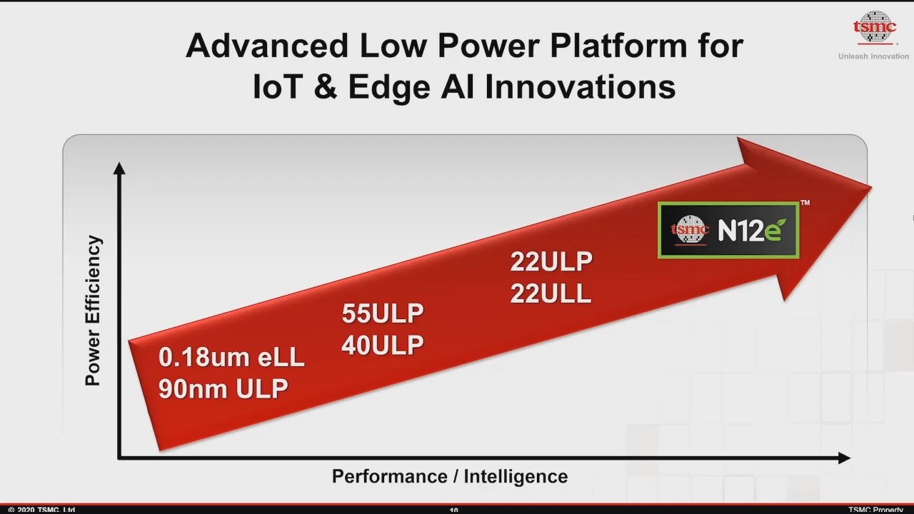
For analog, TSMC has offerings on 22nm (22 Ultra-Low-Leakage), and is currently in the process of developing its N12e (efficient) offerings for this space. N12e will be a dedicated process node covering a lot of the IoT space as well.
Other highlights include TSMC’s CMOS Image Sensing (CIS) nodes, which a number of high-profile camera sensor modules use. Moving from 40nm to 28nm will allow TSMC to offer 0.7 micron pixels and increase overall image sensor size, with TSMC expecting to work with partners to offer 100 megapixel sensors in 2020. On the MEMs side, TSMC is moving from 8-inch wafers to 12-inch wafers, and for High Voltage applications TSMC is investing in its Wafer-on-Wafer bonding options at 28nm.
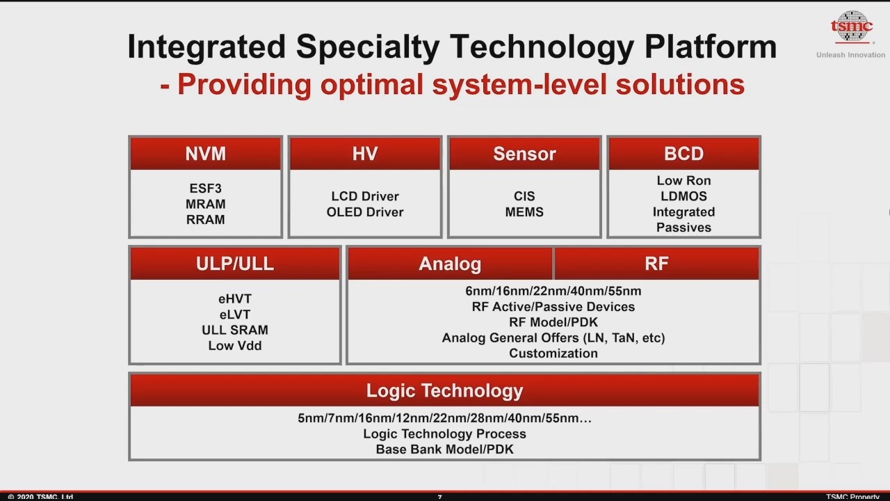
TSMC calls its non-logic business as its ‘specialty’ portfolio, which it says has increased in revenue at 17% CAGR since 2014. Its own capacity for specialty technology has grown 10% Year on Year when comparing equivalent wafer starts, and specialty products now account for 54% of the company’s production on 28nm and above.
Related Reading
- TSMC Details 3nm Process Technology: Full Node Scaling for 2H22 Volume Production
- TSMC To Build 5nm Fab In Arizona, Set To Come Online In 2024
- TSMC & Broadcom Develop 1,700 mm2 CoWoS Interposer: 2X Larger Than Reticles
- TSMC Boosts CapEx by $1 Billion, Expects N5 Node to Be Major Success
- Early TSMC 5nm Test Chip Yields 80%, HVM Coming in H1 2020
- TSMC: 5nm on Track for Q2 2020 HVM, Will Ramp Faster Than 7nm
- TSMC: N7+ EUV Process Technology in High Volume, 6nm (N6) Coming Soon


2 Comments
View All Comments
alexgambler - Wednesday, October 28, 2020 - link
One of the biggest advantages for a person in the university is the price of some of these models. Tuition is truly expensive, and saving a couple of hundred dollars is always nice. For this reason, Lenovo Yoga Tab 3 Pro https://yarkoweb.com/best-tablet-for-students/ and Huawei MediaPad M5 are the most affordable ones. Depending on your personal preferences regarding the performance, display size, and accessories such as pens and keyboards, you might choose the most suitable option.dicsintel - Thursday, August 12, 2021 - link
https://www.setbizsolutions.com/https://www.dsdcindia.com/
http://dicsfaridabad.com/