Huawei Mate 10 and Mate 10 Pro Launch on October 16th, More Kirin 970 Details
by Ian Cutress on September 4, 2017 11:00 AM EST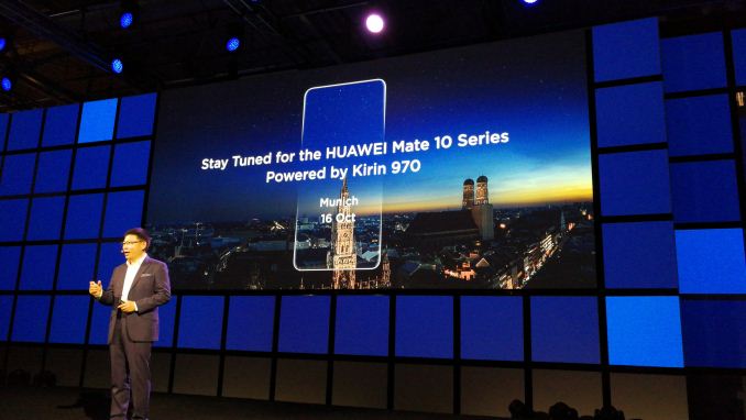
Riding on the back of the ‘not-announced then announced’ initial set of Kirin 970 details, Huawei had one of the major keynote presentations at the IFA trade show this year, detailing more of the new SoC, more into the AI details, and also providing some salient information about the next flagship phone. Richard Yu, CEO of Huawei’s Consumer Business Group (CBG), announced that the Huawei Mate 10 and Mate 10 Pro will be launched on October 16th, at an event in Munich, and will feature both the Kirin 970 SoC and a new minimal-bezel display.
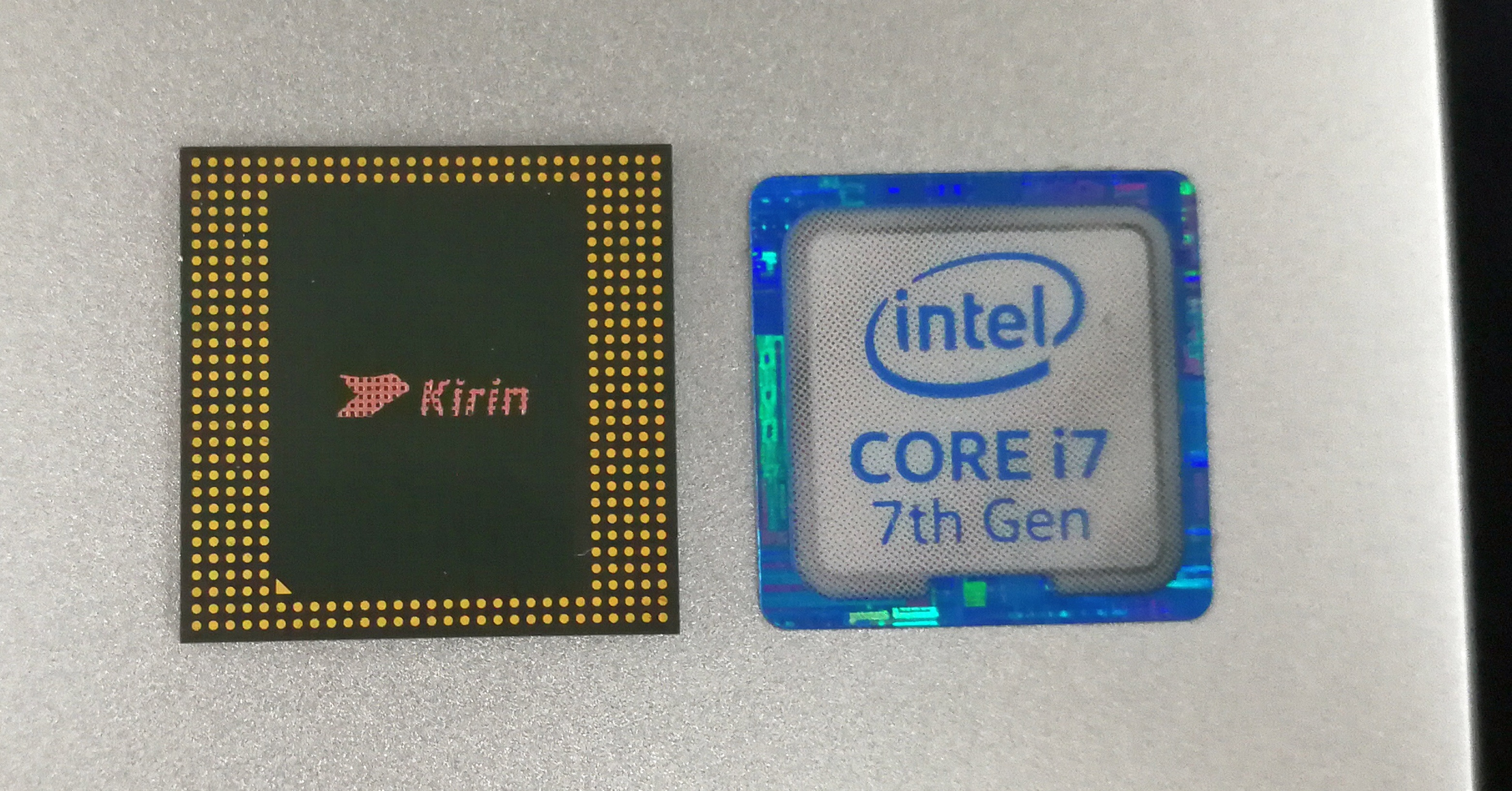
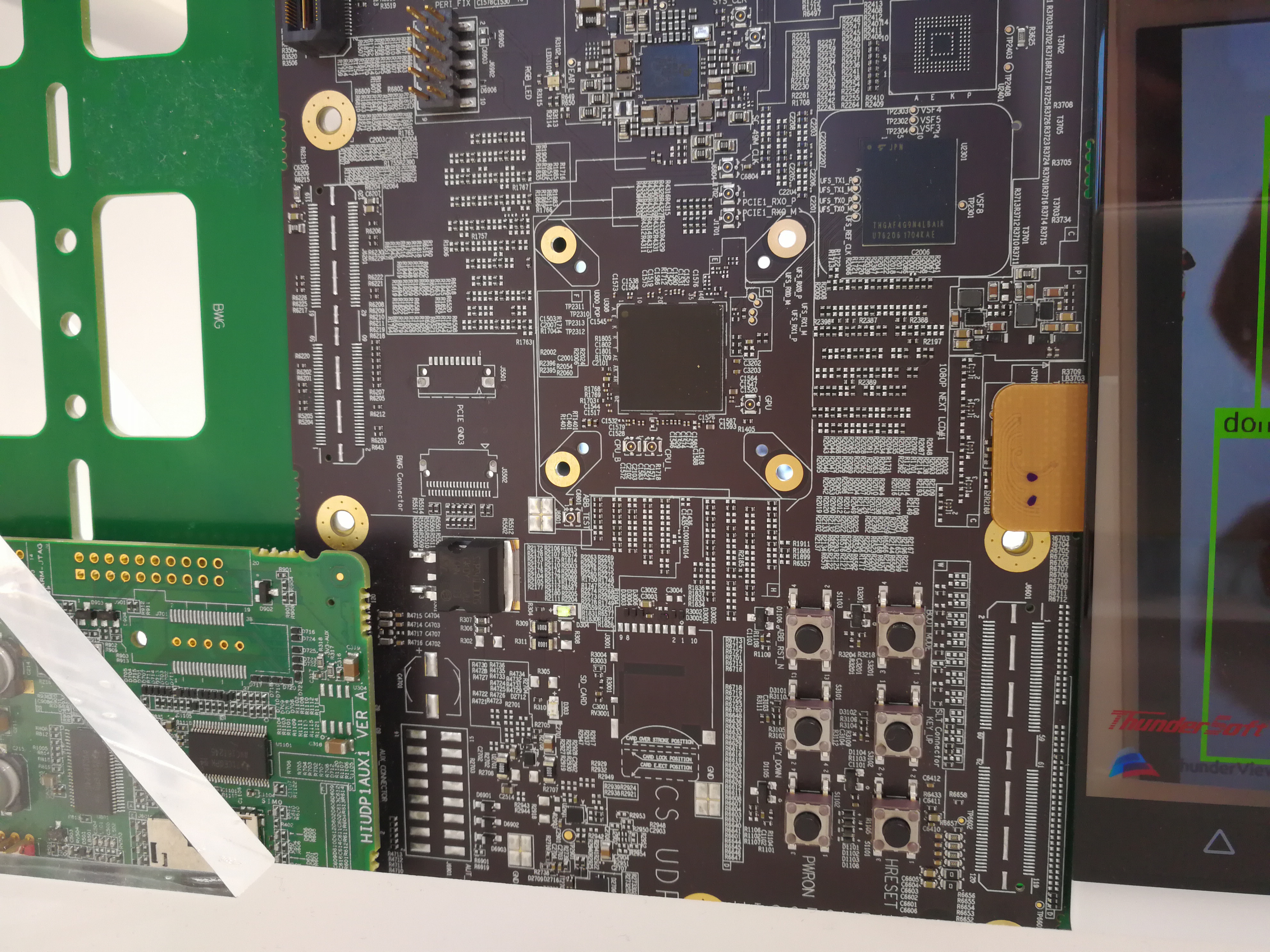
Kirin 970 PCB vs Intel Core i7 Laptop Sticker
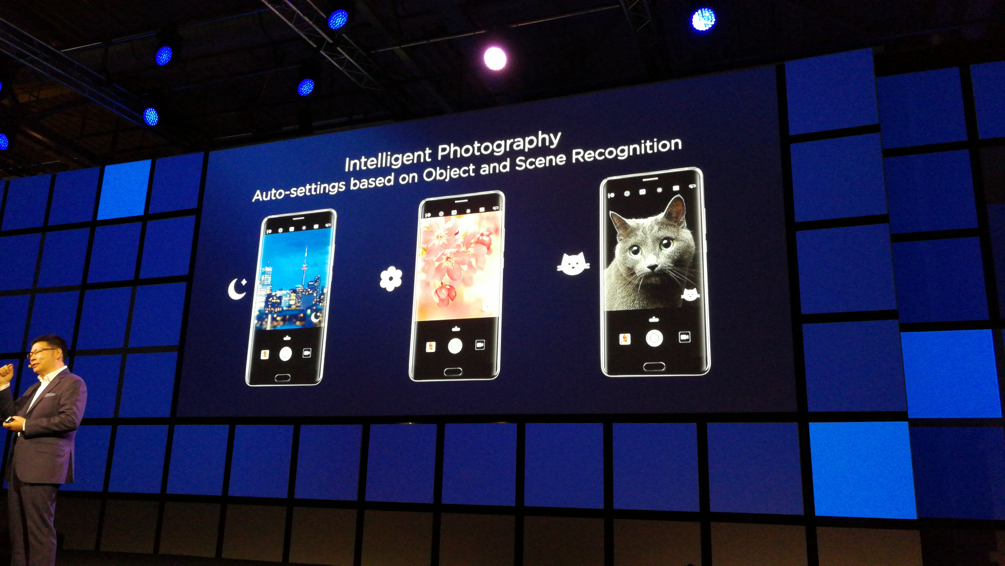
Suffice to say, that is basically all we know about the Mate 10 at this point: a new display technology, and a new SoC with additional AI hardware under-the-hood to start the process of using AI to enhance the experience. When speaking with both Clement Wong, VP of Global Marketing at Huawei, and Christophe Coutelle, Director of Device Software at Huawei, it was clear that they have large, but progressive goals for the direction of AI. The initial steps demonstrated were to assist in providing the best camera settings for a scene by identifying the objects within them – a process that can be accelerated by AI and consume less power. The two from Huawei were also keen to probe the press and attendees at the show about what they thought of AI, and in particular the functions it could be applied to. One of the issues of developing hardware specifically for AI is not really the hardware itself, but the software that uses it.
The Neural Processing Unit (NPU) in the Kirin 970 is using IP from Cambricon Technology (thanks to jjj for the tip, we confirmed it). In speaking with Eric Zhou, Platform Manager for HiSilicon, we learned that the licensing for the IP is different to the licensing agreements in place with, say ARM. Huawei uses ARM core licenses for their chips, which restricts what Huawei can change in the core design: essentially you pay to use ARM’s silicon floorplan / RTL and the option is only one of placement on the die (along with voltage/frequency). With Cambricon, the agreement around the NPU IP is a more of a joint collaboration – both sides helped progress the IP beyond the paper stage with updates and enhancements all the way to final 10nm TSMC silicon.
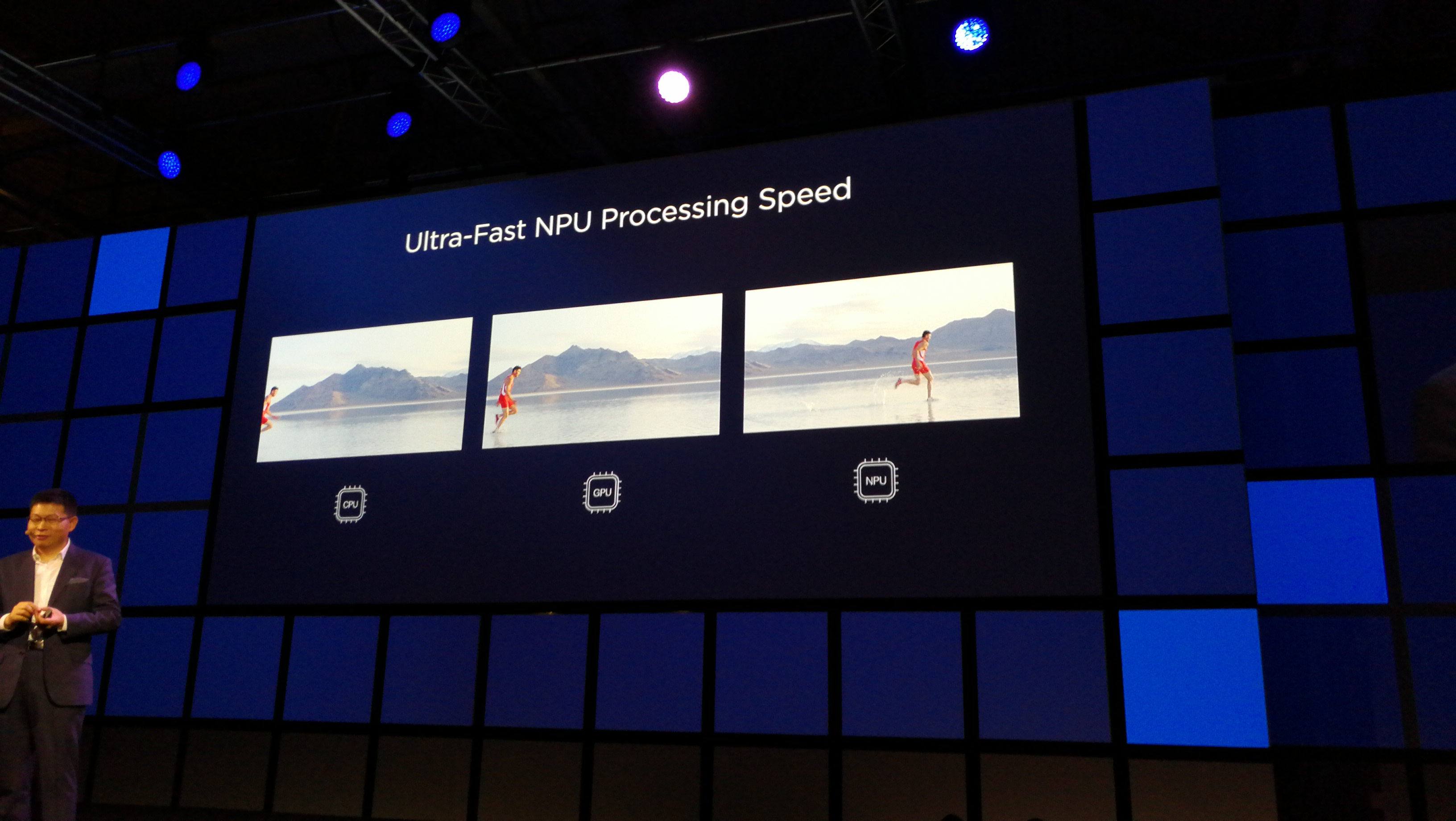
We learned that the IP is scalable, but at this time is only going to be limited to Huawei devices. The configuration of the NPU internally is based on multiple matrix multiply units, similar to that shown in Google’s TPU and NVIDIA’s Tensor core, found in Volta. In Google’s first TPU, designed for neural network training, there was a single 256x256 matrix multiply unit doing the heavy lifting. For the TPUv2, as detailed back at the Hot Chips conference a couple of weeks ago, Google has moved to dual 128x128 matrix multiply units. In NVIDIA’s biggest Volta chip, the V100, they have placed 640 tensor cores each capable of a 4x4 matrix multiply. The Kirin 970 TPU by contrast, as we were told, uses 3x3 matrix multiply units and a number of them, although that number was not provided.
One other element to the NPU that was interesting was that its performance was quoted in terms of 16-bit floating point accuracy. When compared to the other chips listed above, Google’s TPU works best with 8-bit integer math, while Nvidia’s Tensor Core does 16-bit floating point as well. When asked, Eric stated that at this time, FP16 implementation was preferred although that might change, depending on how the hardware is used. As an initial implementation, FP16 was more inclusive of different frameworks and trained algorithms, especially as the NPU is an inference-only design.
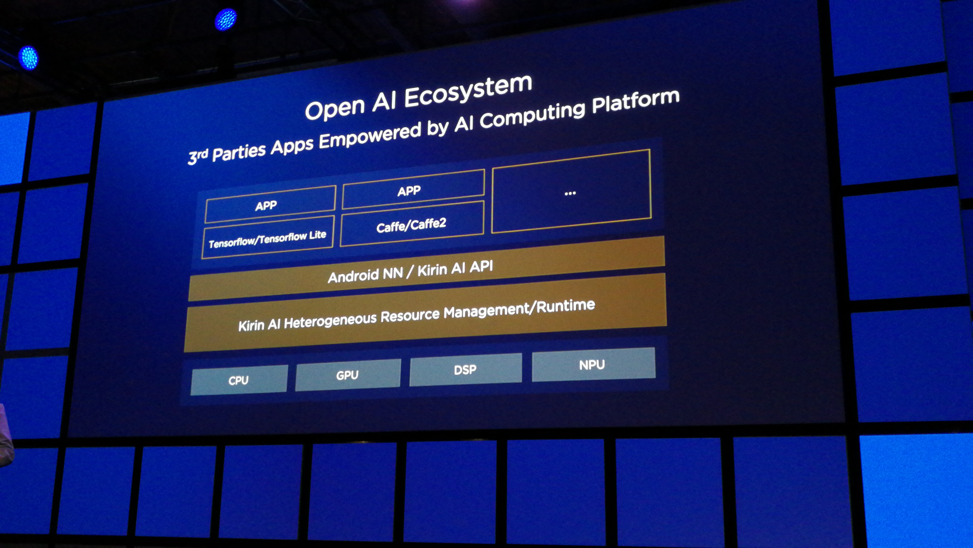
At the keynote, and confirmed in our discussions after, Huawei stated that the API to use the NPU will be available for developers. The unit as a whole will support the TensorFlow and TensorFlow Lite frameworks, as well as Caffe and Caffe2. The NPU can be accessed via Huawei’s own Kirin AI API, or Android’s NN API, relying on Kirin’s AI Heterogeneous Resource Management tools to split the workloads between CPU, GPU, DSP and NPU. I suspect we’ll understand more about this nearer to the launch. Huawei did specifically state that this will be an ‘open architecture’, but failed to mention exactly what that meant in this context.
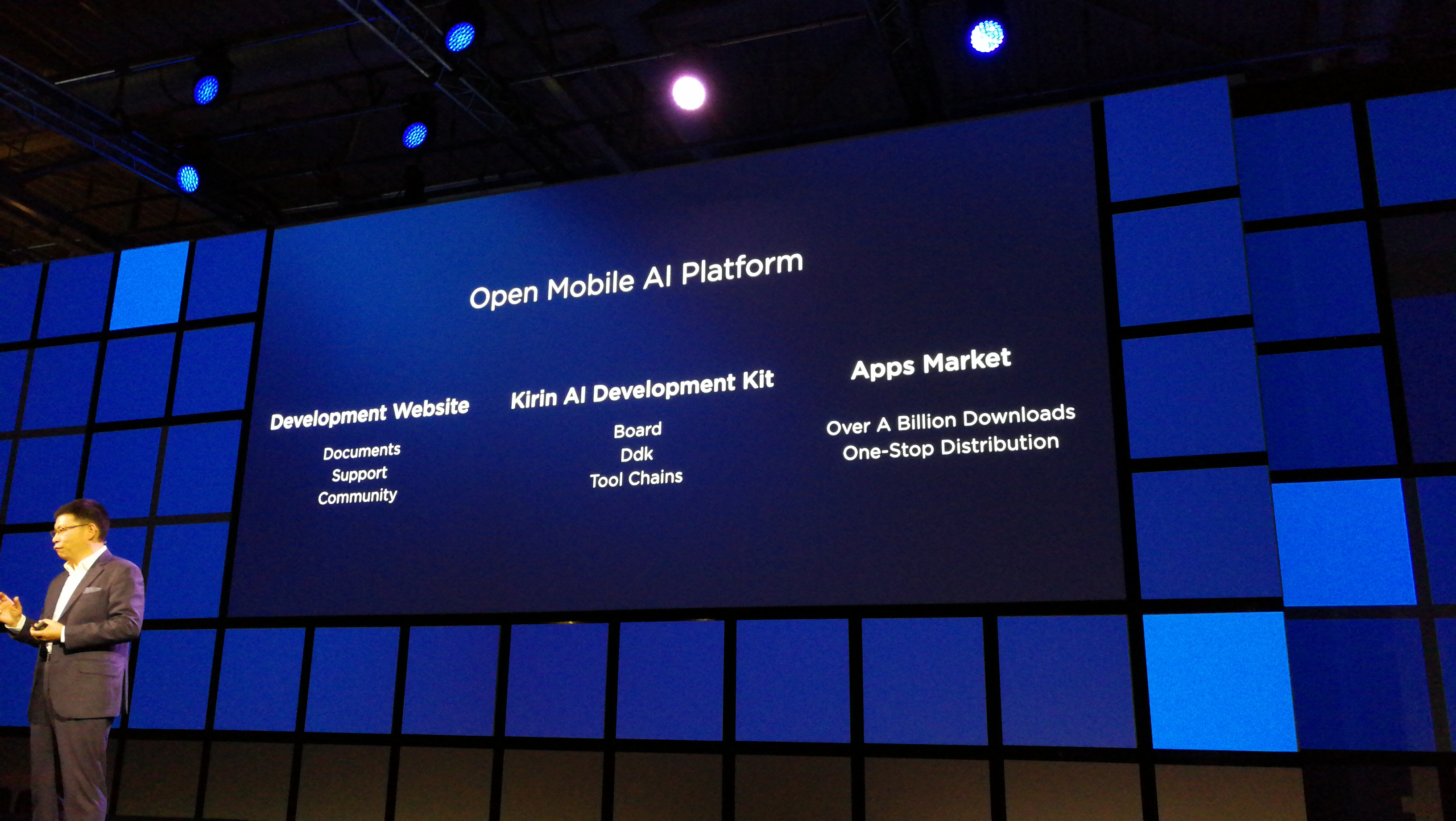
The Kirin 970 will be available on a development board/platform for other engineers and app developers in early Q1, similar to how the Kirin 960 was also available. This will also include a community, support, dedicated tool chains and a driver development kit.
We did learn that the NPU is the size of ‘half a core’, although it was hard to tell if this was ‘half of a single core (an A73 or an A53)’ or ‘half of the cores (all the cores put together)’. We did confirm that the die size is under 100mm2, although an exact number was not provided. It does give a transistor density of 55 million transistors per square mm, which is double what we see on AMD’s Ryzen CPU (25m per mm2) on GloFo 14nm vs TSMC 10nm. We were told that the NPU has its own power domain, and can be both frequency gated and power gated, although during normal operation it will only be frequency gated to improve response time from idle to wake up. Power consumption was not explicitly stated (‘under 1W’), but they did quote that a test of 1000 images being recognized drained a 4000 mAh battery by 0.19%, fluctuating between 0.25W and 0.67W.

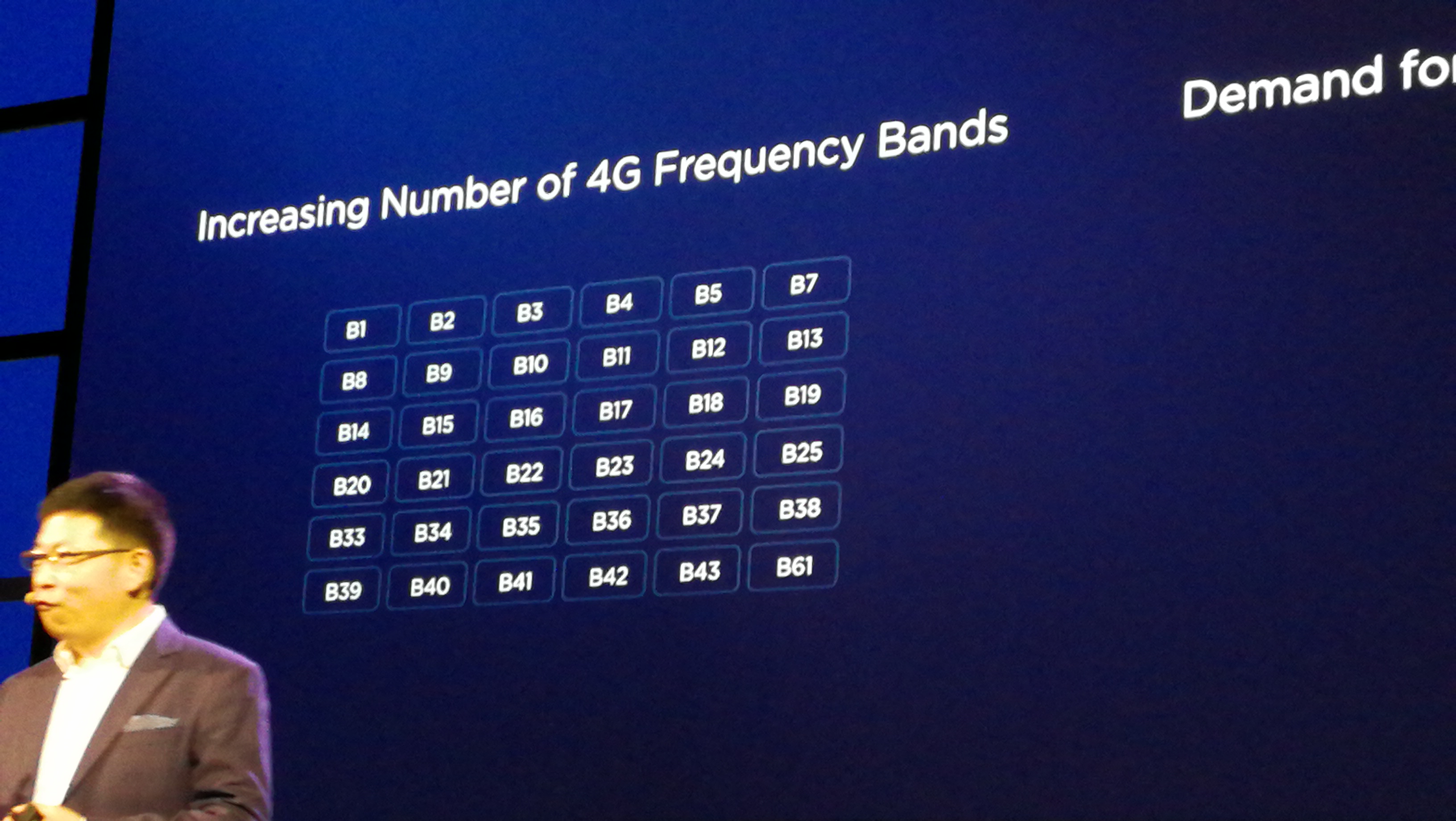
We did draw a few more specifications on the Kirin 970 out of senior management unrelated to the NPU. The display controller can support a maximum screen size of 4K, and the Kirin 970 will support two SIM cards at 4G speeds at the same time, using a time mux strategy. While the model is rated for Category 18 for downloads, giving 1.2 Gbps with 3x carrier aggregation, 4x4 MIMO and 256-QAM, the chip will do Category 13 downloads (up to 150 Mbps). The chip can handle VoLTE on both SIMs as well. Band support is substantial, given in the list below.
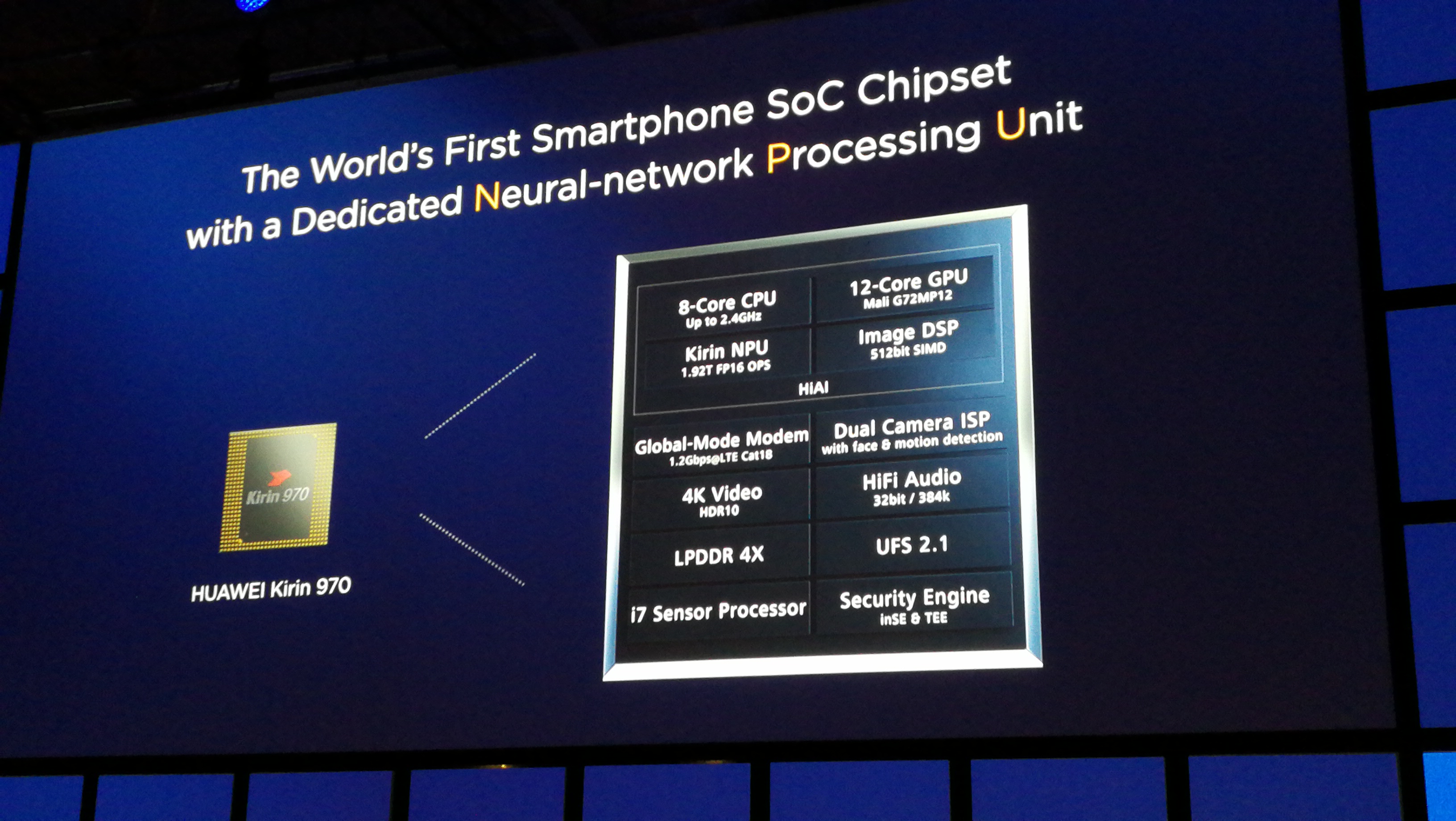
Audio is an odd one out here, with the onboard audio rated to 32-bit and 384 kHz (although SNR will depend on the codec). That’s about 12-15 bits higher than needed and easily multiple times the human sampling rate, but high numbers are seemingly required. The storage was confirmed as UFS 2.1, with LPDDR4X-1833 for the memory, and the use of a new i7 sensor hub.
| HiSilicon High-End Kirin SoC Lineup | |||
| SoC | Kirin 970 | Kirin 960 | Kirin 950/955 |
| CPU | 4x A73 @ 2.40 GHz 4x A53 @ 1.80 GHz |
4x A73 @ 2.36GHz 4x A53 @ 1.84GHz |
4x A72 @ 2.30/2.52GHz 4x A53 @ 1.81GHz |
| GPU | ARM Mali-G72MP12 ? MHz |
ARM Mali-G71MP8 1037MHz |
ARM Mali-T880MP4 900MHz |
| LPDDR4 Memory |
2x 32-bit LPDDR4 @ 1833 MHz |
2x 32-bit LPDDR4 @ 1866MHz 29.9GB/s |
2x 32-bit LPDDR4 @ 1333MHz 21.3GB/s |
| Interconnect | ARM CCI | ARM CCI-550 | ARM CCI-400 |
| Storage | UFS 2.1 | UFS 2.1 | eMMC 5.0 |
| ISP/Camera | Dual 14-bit ISP | Dual 14-bit ISP (Improved) |
Dual 14-bit ISP 940MP/s |
| Encode/Decode | 2160p60 Decode 2160p30 Encode |
2160p30 HEVC & H.264 Decode & Encode 2160p60 HEVC Decode |
1080p H.264 Decode & Encode 2160p30 HEVC Decode |
| Integrated Modem | Kirin 970 Integrated LTE (Category 18) DL = 1200 Mbps 3x20MHz CA, 256-QAM UL = 150 Mbps 2x20MHz CA, 64-QAM |
Kirin 960 Integrated LTE (Category 12/13) DL = 600Mbps 4x20MHz CA, 64-QAM UL = 150Mbps 2x20MHz CA, 64-QAM |
Balong Integrated LTE (Category 6) DL = 300Mbps 2x20MHz CA, 64-QAM UL = 50Mbps 1x20MHz CA, 16-QAM |
| Sensor Hub | i7 | i6 | i5 |
| NPU | Yes | No | No |
| Mfc. Process | TSMC 10nm | TSMC 16nm FFC | TSMC 16nm FF+ |


12 Comments
View All Comments
SydneyBlue120d - Monday, September 4, 2017 - link
Are memory, interconnect and ISP inverted in the chart?jjj - Monday, September 4, 2017 - link
It was public info that they use Cambricon.BTW there is also NovuMind trying to do AI at the edge.http://www.eetimes.com/document.asp?doc_id=1332226
Infy2 - Monday, September 4, 2017 - link
Hopefully with Mate 10 Huawei would finally to pay some attention to display calibration.ToTTenTranz - Monday, September 4, 2017 - link
"It does give a transistor density of 55 million transistors per square mm, which is double what we see on AMD’s Ryzen CPU (25m per mm2) on 16FF+ vs 10nm."AMD's Ryzen is built on GlobalFoundries' 14LPP, not TSMC's 16FF+.
boozed - Monday, September 4, 2017 - link
"Kirin 970 PCB [sic] vs Intel Core i7 Laptop Sticker"A little help for those of us who don't have any Intel Core i7 Laptop Stickers handy...
Drumsticks - Tuesday, September 5, 2017 - link
This sounds like an interesting SoC. Huawei's phones are generally available overseas, right?Also, very very minor correction: a Tensor core in GV100 does 4x4x4 matrix multiplication, not 4x4.
twotwotwo - Tuesday, September 5, 2017 - link
Dunno much about these areas, but if I'm recalling high school math right, I think there are 6.3M times more scalar multiplies in a 128x128 matrix multiply (like Google's TPU does) than in a 3x3 one. (A dot product for each position in the output matrix, so 128**3/3**3.) It's not that TPUs were for training, either; as I understand it they were for executing already-trained networks.FP16 3x3 matrix stuff makes me of convolutional image filters, particularly since a lot of the focus in the chip is on image processing. Maybe this is mostly exposing and slickly rebranding hardware they had anyway for the ISP and other traditional graphics stuff? Of course, if it turns out they've pulled something useful out of that I'll be impressed anyway.
twotwotwo - Tuesday, September 5, 2017 - link
Sorry, 77K not 6.3M! Sigh.Santoval - Wednesday, September 6, 2017 - link
"It does give a transistor density of 55 million transistors per square mm, which is double what we see on AMD’s Ryzen CPU (25m per mm2) on GloFo 14nm vs TSMC 10nm."Not bad at all. I thought TSMC 10nm had roughly the same transistor density as Intel 14nm (which has 37.5 million transistors per mm^2, with Intel 10nm having reached 100.8 million per mm^2), but it is more likely equivalent to an Intel ~13nm process. As for GloFo, if they managed to quadruple their transistor density in their 7nm node (as the 14 --> 7nm transition implies) it would almost precisely match that of Intel 10nm's, but I highly doubt they will - thought I hope they do. At most I expect they will manage a 3x transistor density, i.e. around 75 million transistors per mm^2.
Soundgardener - Thursday, September 14, 2017 - link
"riding on the back of the not-announced then announced"Products are commonly characterized as 'not-announced' prior to announcement, and 'announced' afterwards. However, convention notwithstanding, thanks for clarifying that this is indeed the case in this instance; it's comforting to know some things still work as expected, in the topsy turvey hoi poloy everyday rat-race zeitgeist of out current modern paradigm that we call 'life'.
I shall approach the rest of my week with renewed vigour and fortification, maybe even zeal*.
Disclaimer: I live in New Zealand, which complicates matters.