Canon
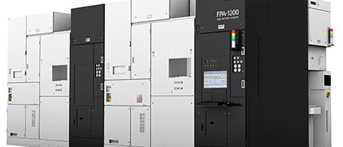
Canon has recently revealed its FPA-1200NZ2C, a nanoimprint semiconductor manufacturing tool that can be used to make advanced chips. The device uses nanoimprint lithography (NIL) technology as an alternative to photolithography, and can theoretically challenge extreme ultraviolet (EUV) and deep ultraviolet (DUV) lithography tools when it comes to resolution. Unlike traditional DUV and EUV photolithography equipment that transfers a circuit pattern onto a resist-coated wafer through projection, nanoimprint tool employs a different technique. It uses a mask, embossed with the circuit pattern, which directly presses against the resist on the wafer. This method eliminates the need for an optical mechanism in the pattern transfer process, which promises a more accurate reproduction of intricate circuit patterns from the mask to the wafer. In theory, NIL enables...


