Arm Announces Mobile Armv9 CPU Microarchitectures: Cortex-X2, Cortex-A710 & Cortex-A510
by Andrei Frumusanu on May 25, 2021 9:00 AM EST- Posted in
- SoCs
- CPUs
- Arm
- Smartphones
- Mobile
- Cortex
- ARMv9
- Cortex-X2
- Cortex-A710
- Cortex-A510
The Cortex-X2: More Performance, Deeper OoO
We first start off with the Cortex-X2, successor to last year’s Cortex-X1. The X1 marked the first in a new IP line-up from Arm which diverged its “big” core offering into two different IP lines, with the Cortex-A sibling continuing Arm’s original design philosophy of PPA, while the X-cores are allowed to grow in size and power in order to achieve much higher performance points.
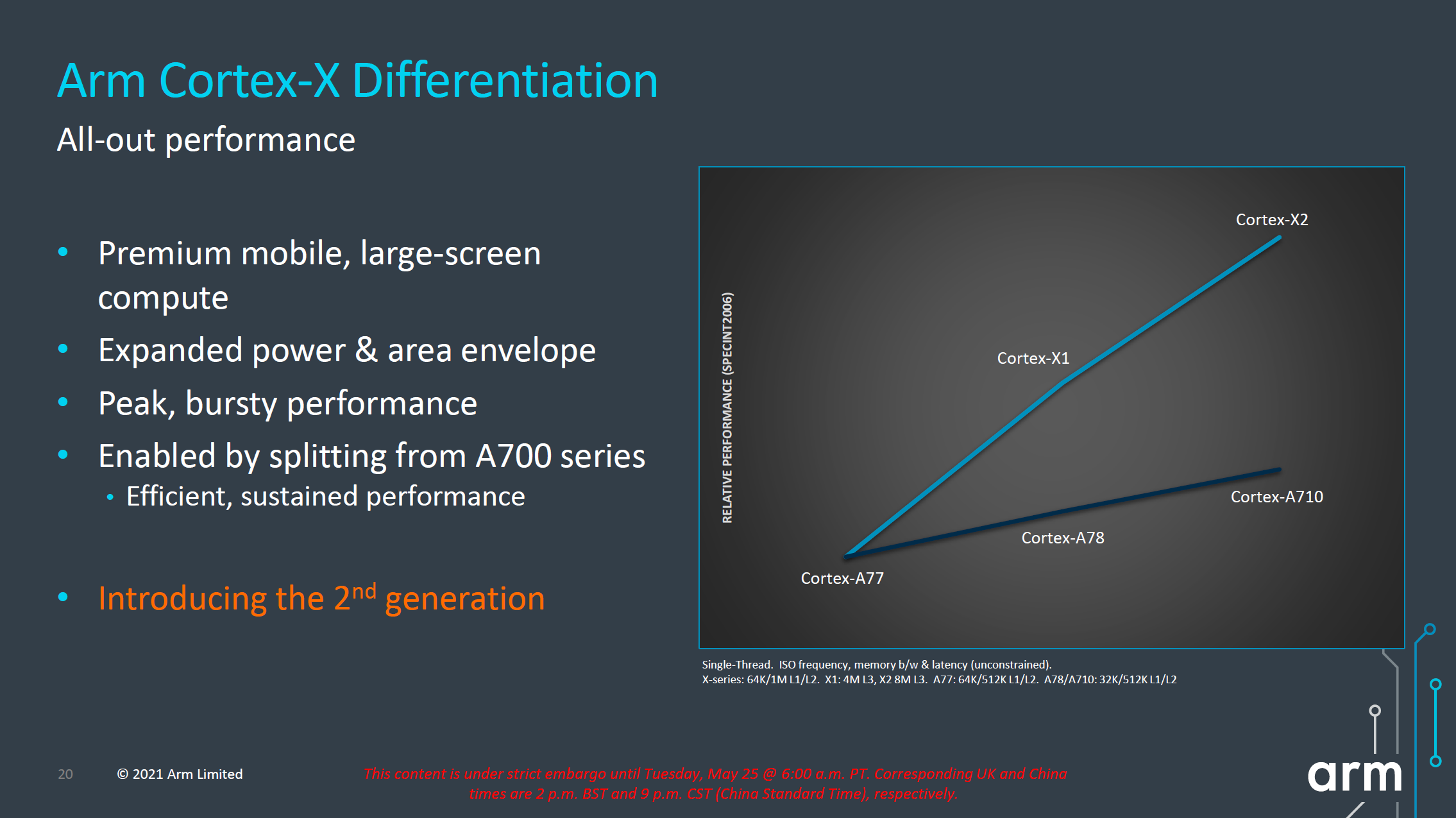
The Cortex-X2 continues this philosophy, and further grows the performance and power gap between it and its “middle” sibling, the Cortex-A710. I also noticed that throughout Arm’s presentation there were a lot more mentions of having the Cortex-X2 being used in larger-screen compute devices and form-factors such as laptops, so it might very well be an indication of the company that some of its customers will be using the X2 more predominantly in such designs for this generation.
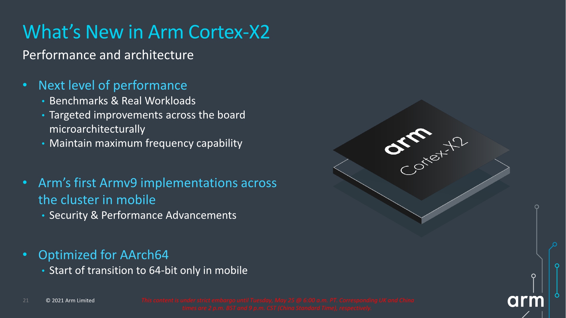
From an architectural standpoint the X2 is naturally different from the X1, thanks in large part to its support for Armv9 and all of the security and related ISA platform advancements that come with the new re-baselining of the architecture.
As noted in the introduction, the Cortex-X2 is also a 64-bit only core which only supports AArch64 execution, even in PL0 user mode applications. From a microarchitectural standpoint this is interesting as it means Arm will have been able to kick out some cruft in the design. However as the design is a continuation of the Austin family of processors, I do wonder if we’ll see more benefits of this deprecation in future “clean-sheet” big cores designs, where AArch64-only was designed from the get-go. This, in fact, is something that's already happening in other members of Arm's CPU cores, as the new little core Cortex-A510 was designed sans-AArch32.
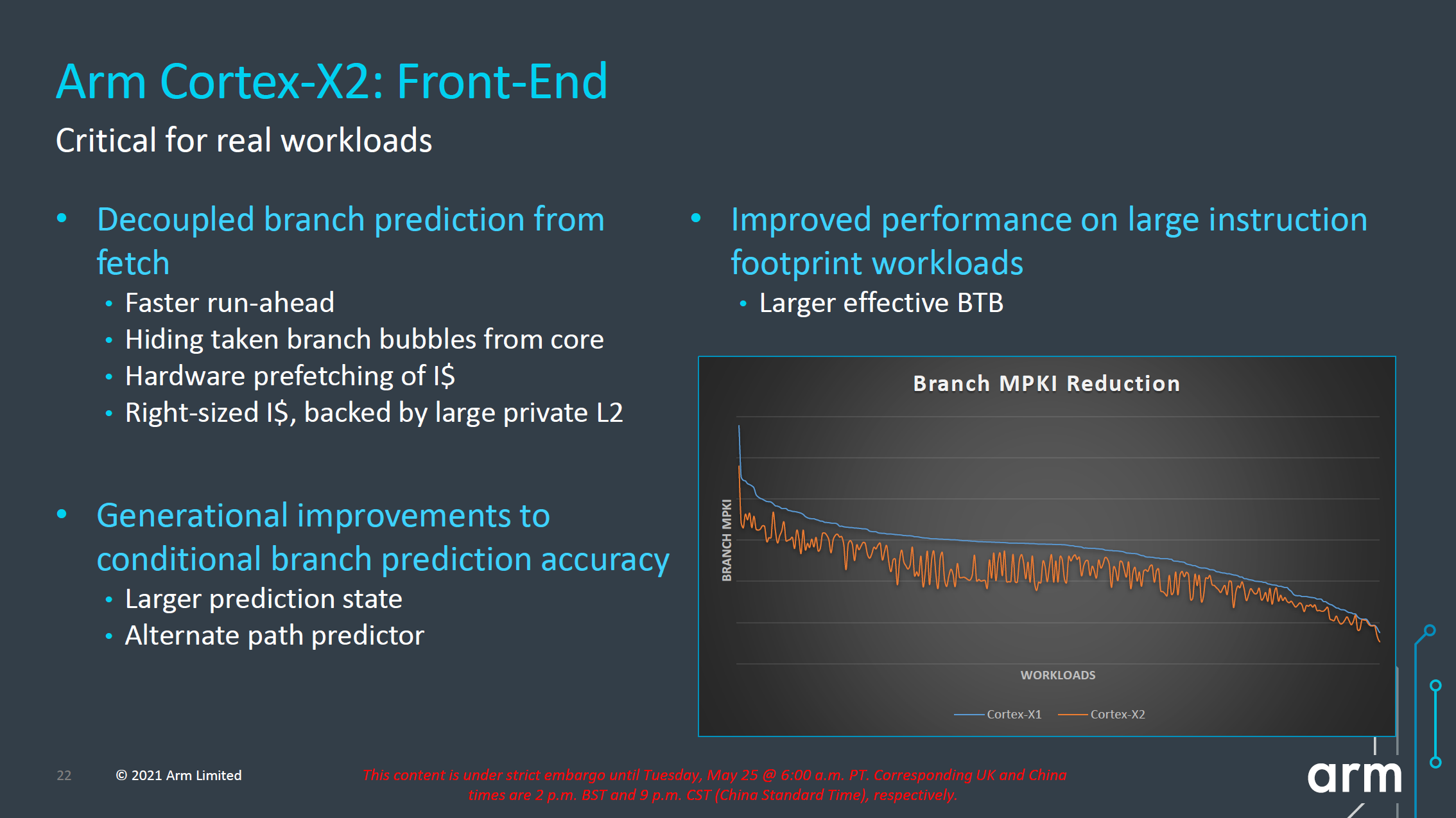
Starting off with the front-end, in general, Arm has continued to try to improve what it considers the most important aspect of the microarchitecture: branch prediction. This includes continuing to run the branch resolution in a decoupled way from the fetch stages in order to being able to have these functional blocks be able to run ahead of the rest of the core in case of mispredicts and minimize branch bubbles. Arm generally doesn’t like to talk too much details about what exactly they’ve changed here in terms of their predictors, but promises a notable improvement in terms of branch prediction accuracy for the new X2 and A710 cores, effectively reducing the MPKI (Misses per kilo instructions) metric for a very wide range of workloads.
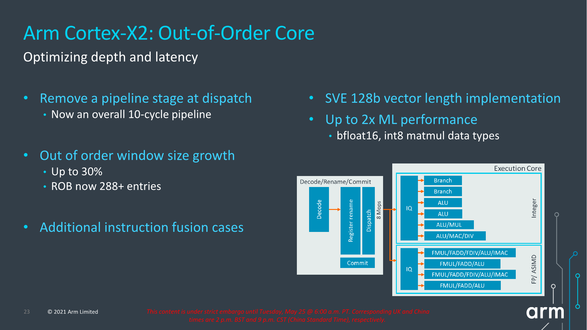
The new core overall reduces its pipeline length from 11 cycles to 10 cycles as Arm has been able to reduce the dispatch stages from 2-cycles to 1-cycle. It’s to be noted that we have to differentiate the pipeline cycles from the mispredict penalties, the latter had already been reduced to 10 cycles in most circumstances in the Cortex-A77 design. Removing a pipeline stage is generally a rather large change, particularly given Arm’s target of maintaining frequency capabilities of the core. This design change did incur some more complex engineering and had area and power costs; but despite that, as Arm explains in, cutting a pipeline stage still offered a larger return-on-investment when it came to the performance benefits, and was thus very much worth it.
The core also increases its out-of-order capabilities, increasing the ROB (reorder buffer) by 30% from 224 entries to 288 entries this generation. The effective figure is actually a little bit higher still, as in cases of compression and instruction bundling there are essentially more than 288 entries being stored. Arm says there’s also more instruction fusion cases being facilitated this generation.
On the back-end of the core, the big new change is on the part of the FP/ASIMD pipelines which are now SVE2-capable. In the mobile space, the SVE vector length will continue to be 128b and essentially the new X2 core features similar throughput characteristics to the X1’s 4x FP/NEON pipelines. The choice of 128b vectors instead of something higher is due to the requirement to have homogenous architectural feature-sets amongst big.LITTLE designs as you cannot mix different vector length microarchitectures in the same SoC in a seamless fashion.
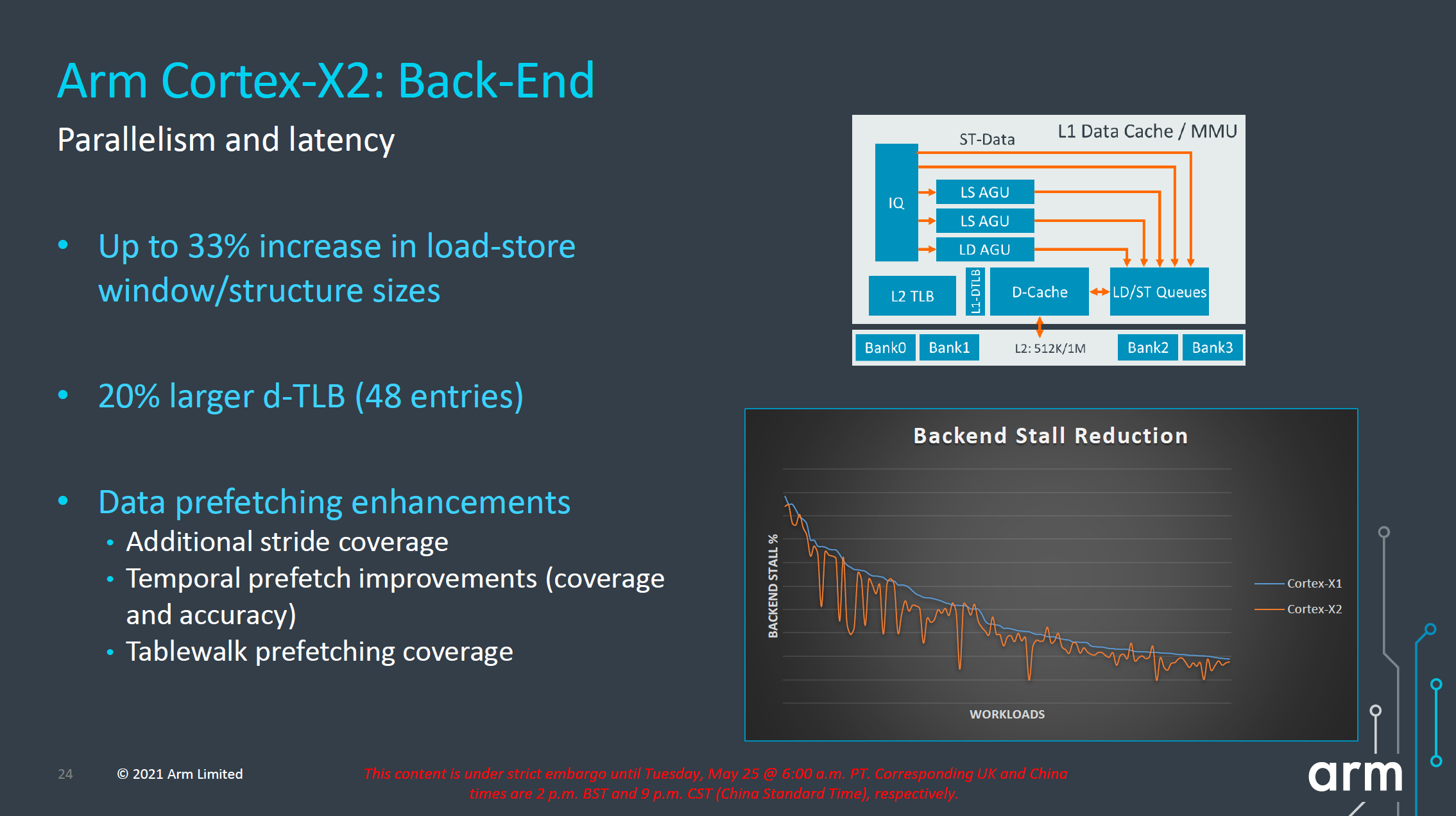
On the back-end, the Cortex-X2 continues to focus on increasing MLP (memory level parallelism) by increasing the load-store windows and structure sizes by 33%. Arm here employs several structures and generally doesn’t go into detail about exactly which queues have been extended, but once we get our hands on X2 systems we’ll be likely be able to measure this. The L1 dTLB has grown from 40 entries to 48 entries, and as with every generation, Arm has also improved their prefetchers, increasing accuracies and coverage.
One prefetcher that surprised us in the Cortex-X1 and A78 earlier this year when we first tested new generation devices was a temporal prefetcher – the first of its kind that we’re aware of in the industry. This is able to latch onto arbitrary repeated memory patterns and recognize new iterations in memory accesses, being able to smartly prefetch the whole pattern up to a certain depth (we estimate a 32-64MB window). Arm states that this coverage is now further increased, as well as the accuracy – though again the details we’ll only able to see once we get our hands on silicon.
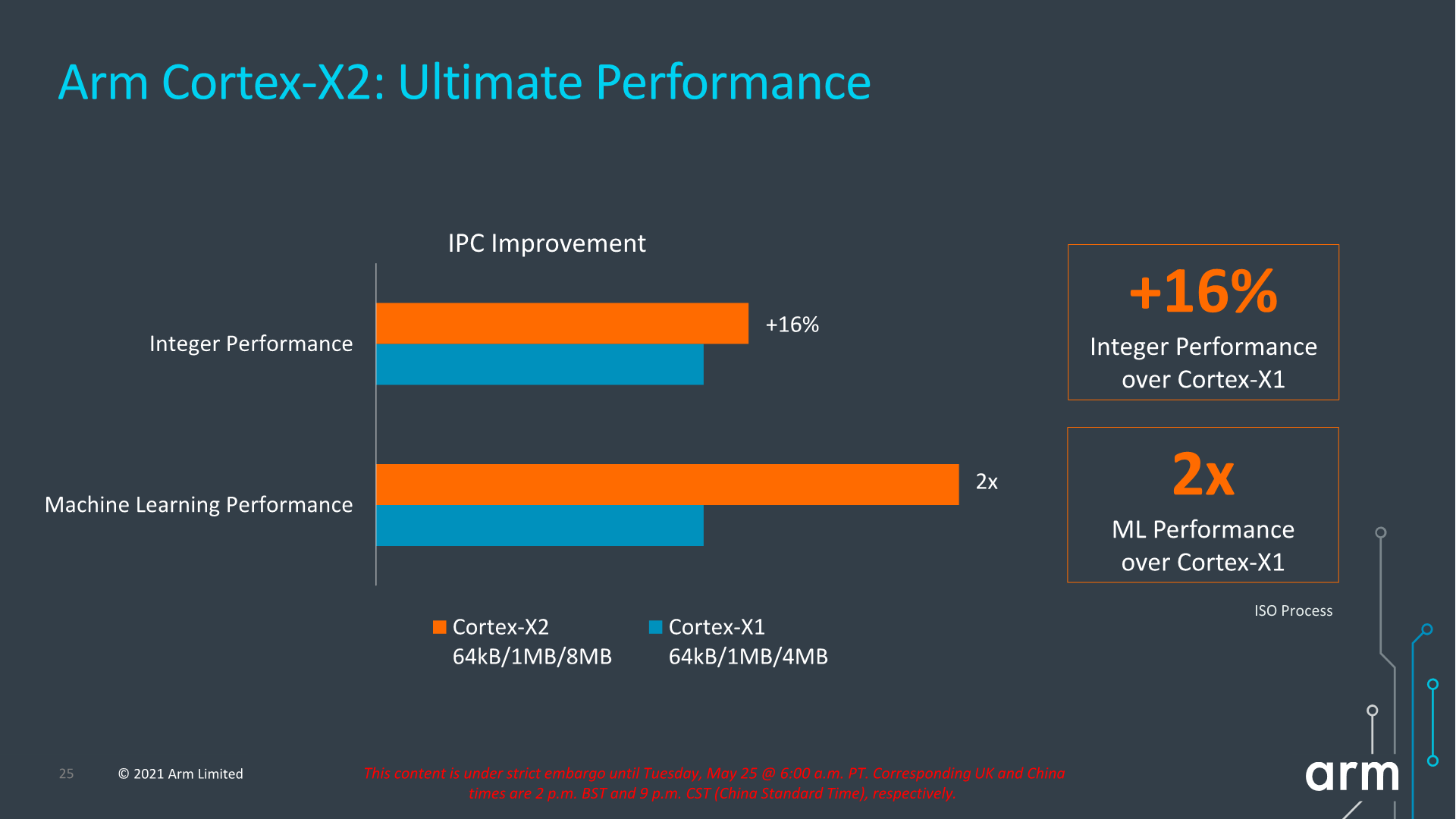
In terms of IPC improvements, this year’s figures are quoted to reach +16% in SPECint2006 at ISO frequency. The issue with this metric (and which applies to all of Arm’s figures today) is that Arm is comparing an 8MB L3 cache design to a 4MB L3 design, so I expect a larger chunk of that +16% figure to be due to the larger cache rather than the core IPC improvements themselves.
For their part, Arm is reiterating that they're expecting 8MB L3 designs for next year’s X2 SoCs – and thus this +16% figure is realistic and is what users should see in actual implementations. But with that said, we had the same discussion last year in regards to Arm expecting 8MB L3 caches for X1 SoCs, which didn't happen for either the Exynos 2100 nor the Snapdragon 888. So we'll just have to wait and see what cache sizes the flagship commercial SoCs end up going with.

In terms of the performance and power curve, the new X2 core extends itself ahead of the X1 curve in both metrics. The +16% performance figure in terms of the peak performance points, though it does come at a cost of higher power consumption.
Generally, this is a bit worrying in context of what we’re seeing in the market right now when it comes to process node choices from vendors. We’ve seen that Samsung’s 5LPE node used by Qualcomm and S.LSI in the Snapdragon 888 and Exynos 2100 has under-delivered in terms of performance and power efficiency, and I generally consider both big cores' power consumption to be at a higher bound limit when it comes to thermals. I expect Qualcomm to stick with Samsung foundry in the next generation, so I am admittedly pessimistic in regards to power improvements in whichever node the next flagship SoCs come in (be it 5LPP or 4LPP). It could well be plausible that we wouldn’t see the full +16% improvement in actual SoCs next year.


181 Comments
View All Comments
jeremyshaw - Tuesday, May 25, 2021 - link
Something I'm not quite catching with the DSU, does it allow for different configurations that we've already seen? Something like the 8xA78C we saw announced a while back?jeremyshaw - Tuesday, May 25, 2021 - link
*than, sorrySarahKerrigan - Tuesday, May 25, 2021 - link
They show 8x X2 configs, so I'd be shocked if 8xA710 was not also on the menu.igor velky - Tuesday, May 25, 2021 - link
first two slides on page 5 will give you answer,both slides show cpu cores inside one cpu cluster
first slide shows different cores,
second shows only one type of core in cpu cluster
on page 6 because of bad formatting there are two slides looking like one picture
so second slide, bottom half of first picture
shows you that you can put max 8 cpu clusters to one chip.
so you can have
max 8 cpu cores per cpu cluster
times
8 cpu clusters per one chip.
you choose cores, you choose how many cores, you choose which type of cores, you choose how many memory channels, you choose how many and what type of additional accelerators you put inside chip...
because youre apple, samsung, qualcomm...
and you choose this things and let someone to "etch it" into silicon.
and you then sell it.
melgross - Tuesday, May 25, 2021 - link
Well, Apple doesn’t “choose” cores, they design them from scratch.Linustechtips12#6900xt - Wednesday, May 26, 2021 - link
ehhh, they get the IP for cores like the x1 or a76 then they tweak them either a lot or a little and create their current "firestorm/Icestorm" coresmichael2k - Wednesday, May 26, 2021 - link
Sure, they tweak them a lot, just like I tweaked your post a lot to make my own. The A13 released in 2019 was an 8 wide CPU; in comparison the state of the art A76 at the time was only a 4 wide CPU. That’s a pretty big deal.The X1 has an 8 wide dispatch, meaning it can issue 8 Mops per cycle but only decode 5 instructions per cycle. This is 2 years after Apple released the A13 which was 8 wide dispatch and decode. If you look at Anandtech’s A14 article you see that Apple has made the Icestorm cores roughly equivalent to an A76 since it is a 3 wide out of order design.
You can read more here:
https://www.anandtech.com/show/16226/apple-silicon...
mattbe - Wednesday, May 26, 2021 - link
This is complete BS. They license the ISA from ARM. They DO NOT USE OR TWEAK cores like the X1 and A76 to create their firestorm/ice storm cores. These are information that can easily be verified so it's pretty ignorant for you to make those claims.FunBunny2 - Wednesday, May 26, 2021 - link
" They DO NOT USE OR TWEAK cores"near as I can tell, most 'innovation' in cpu design/engineering has been, for years, throwing ever expanding transistor budgets (can we expect that to continue?) at register width, path width, buffer/cache width and number, pulling off-chip function on-chip. and the like. if Apple should ever publish the full spec of one of these chips, will we see that they've done anything more 'innovative' than Bigger, Wider, More?
all of the 'innovation' cited by michael2k fits that bill.
mode_13h - Thursday, May 27, 2021 - link
> if Apple should ever publish the full spec of one of these chips,> will we see that they've done anything more 'innovative' than Bigger, Wider, More?
You don't get perf/W numbers like Apple's by simply doing "bigger, wider, more".
There's information out there about some of their tricks, if you're willing to look for it. But I understand that it takes work and why do that, when you're perfectly content in your belief that there's nothing new under the sun?