Original Link: https://www.anandtech.com/show/8701/the-google-nexus-9-review
The Google Nexus 9 Review
by Joshua Ho & Ryan Smith on February 4, 2015 8:00 AM EST- Posted in
- HTC
- Project Denver
- Android
- Mobile
- Tablets
- NVIDIA
- Nexus 9
- Lollipop
- Android 5.0
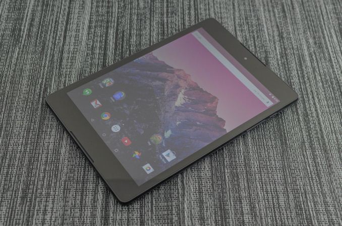
For the past few years, we’ve seen Google place significant emphasis on price as a way of competing with other tablets on the market. The original Nexus 7 managed to deliver a good tablet experience without the conventional 500 USD price for a tablet. The successor to the Nexus 7 was even more incredible, as it pushed hardware that was equal to or better than most tablets on the market at a lower price. However, as with most of these low cost Nexus devices not everything was perfect as corners still had to be cut in order to hit these low price points.
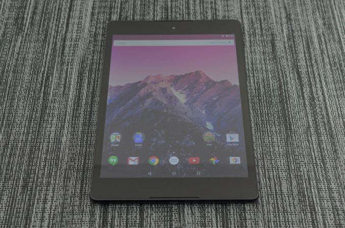
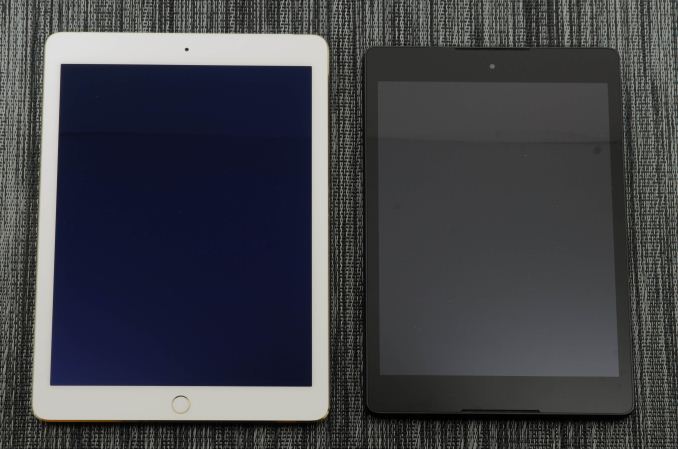
The Nexus 9 is supposed to be the polar opposite. Instead of driving price as the primary differentiator, Google has refocused on the high end tablet market for the Nexus 9. With a new focus on industrial and material design, along with some of the latest and greatest hardware in every dimension. HTC has been brought on as a partner for the first time since the Nexus One to enable this vision. In addition, NVIDIA’s Tegra K1 with Denver CPUs can be found inside as the launch platform for Android Lollipop on 64-bit ARM v8. The Nexus 9 also has a 4:3 aspect ratio on its display, a notable departure from the 16:10 ratio that was shared with phones. There’s also the addition of BoomSound speakers on the front and a metal frame running around the edge of the device for improved in-hand feel. The rest of the key specifications can be found below.
| Nexus 9 | |
| SoC | 2.3GHz 64-bit dual core Tegra K1 Denver SoC |
| RAM/NAND | 2GB LPDDR3 + 16/32GB NAND |
| Display | 8.9" 2048x1536 IPS LCD |
| Network | WiFi only or 2G / 3G / 4G LTE SKU |
| Dimensions | 153.68 x 228.25 x 7.95mm, 425g WiFi, 436g LTE |
| Camera | 8MP Rear Facing (IMX219) with F/2.4 aperture, 1.6MP FFC (OV9760) |
| Battery | 6700 mAh (25.46 Whr) |
| OS | Android 5.0 Lollipop |
| Connectivity | 802.11a/b/g/n/ac + BT 4.1 (BCM4354) , USB2.0, GPS/GNSS, NFC (BCM2079x) |
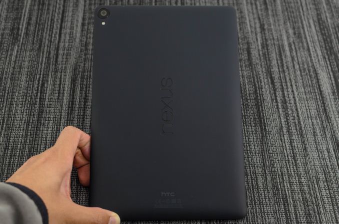
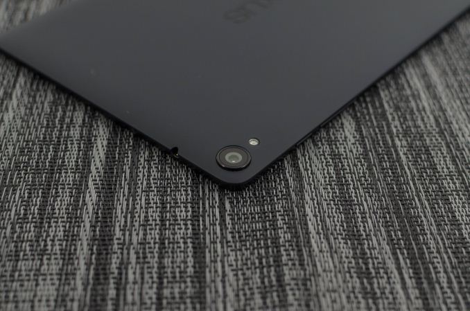
While specs are nice, one of the key areas where the Nexus 9 has to push the limits is in industrial and material design. To this end, Google seems to have mostly delivered, but not quite at the levels that one might have wished. The back continues to be a soft-touch plastic, with almost nothing other than required regulatory text, the Nexus logo, and the camera with its LED flash. I definitely like the feeling of the back cover with its slight outward curve, but on the black model the finish seems to attract smudges quite easily. This is unlikely to be a real problem, but those that are extremely concerned with fingerprint smudges may want to look into getting the white version of this tablet. There is a small amount of give in the dead center of the device, but this is something that one has to actively try to do instead of being immediately obvious. In my experience, the same is true for the Nexus 5 as well which calls into question whether this is a real issue.
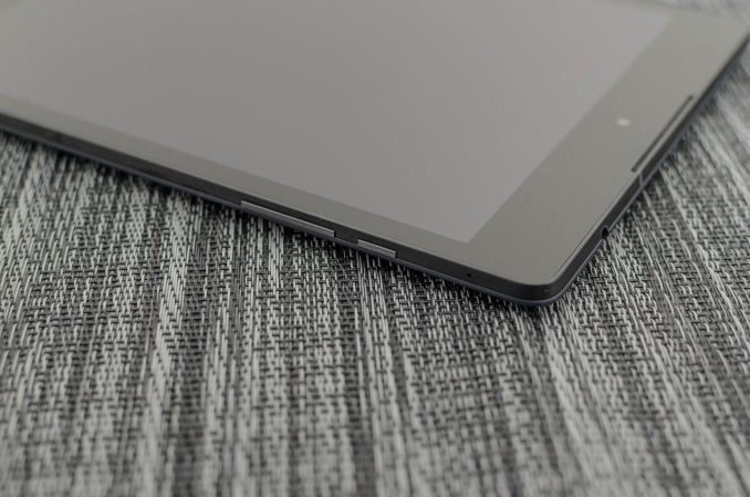
Outside of the back cover, the metal rim definitely makes for a significant contrast in texture and feel. The texture seems to be the same as the M8’s gunmetal grey, with an extremely delicate brushed texture. Unfortunately, this does mean that the metal feels glossy in the hand rather than matte, and I suspect that a more standard matte texture would be better in this case. At any rate, it still feels great to the touch, especially when the device is cold. The metal frame has a noticeable outward angle to it, and does make it feel like the One (M7) in that respect. Along the left side of the rim, the device is barren but there is a microUSB 2 port along the bottom and a hole for one of the microphones on the device. Along the right side, we see another microphone hole, the volume rocker, and the power button. While the feel of the buttons is relatively clicky and the actuation is solid, the buttons are definitely a bit on the thin side and are hard to locate and press. The top side has a 3.5mm jack along the top right, and a single plastic line that breaks up the metal frame in line with the speakers.
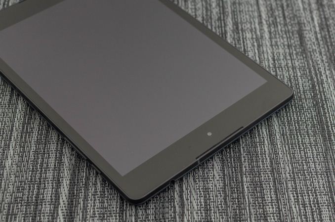
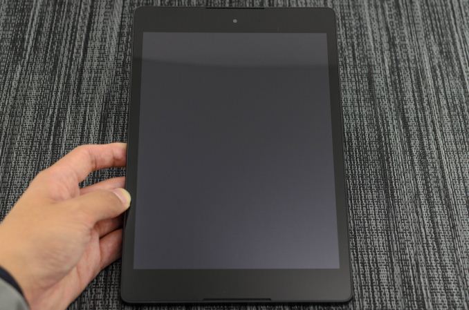
Speaking of the speakers, unlike the One (M8) and (M7) where the front-facing speakers are a major design element, the speakers on the Nexus 9 are noticeably hidden away from view. They’re definitely present, but the speaker grilles are recessed and black to match the bezels. The recessed nature helps with the design minimalism that is pervasive throughout the Nexus 9, but it does mean that it’s pretty easy for lint and dust to find its way into the grilles. There’s also a noticeable lip around the entire display which makes for a noticeable rounded metal edge, which should help to some extent for drop protection although the thickness of the lip is really quite thin. This means that it can only help with drop protection on flat surfaces. Other than the speaker grilles, the front of the tablet is almost barren. There’s a front-facing camera on the top, and a light sensor to the right of this camera. Other than this, there’s only a single LED at the bottom of the device but it appears that this hasn’t been enabled in the system as I only see it active when charging the device from a fully-depleted state.
Overall, the Nexus 9’s build quality is decent. It isn’t quite as incredible as an all-aluminum unibody, but the feel is quite comfortable and the design fits well with the rest of the Nexus line-up. I do wish the metal frame had a bit more matte feel to it and the buttons do need some work, but I otherwise don’t really have a lot to complain about in this device. It is quite obvious that disassembling the device starts with the back cover though, as it’s pretty easy to stick a fingernail between the back cover and metal frame to pry it apart like the One X.
SoC Architecture: NVIDIA's Denver CPU
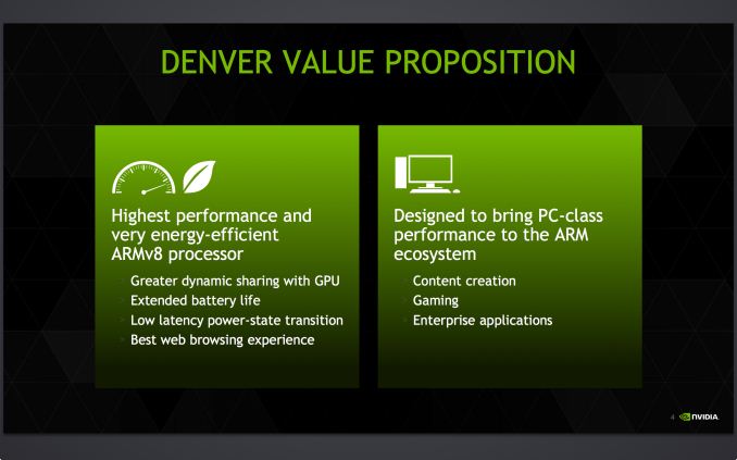
It admittedly does a bit of a disservice to the rest of the Nexus 9 both in terms of hardware and as a complete product, but there’s really no getting around the fact that the highlight of the tablet is its NVIDIA-developed SoC. Or to be more specific, the NVIDIA-developed Denver CPUs within the SoC, and the fact that the Nexus 9 is the first product to ship with a Denver CPU.
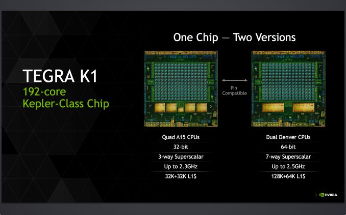
NVIDIA for their part is no stranger to the SoC game, now having shipped 5 generations of Tegra SoCs (with more on their way). Since the beginning NVIDIA has been developing their own GPUs and then integrating those into their Tegra SoCs, using 3rd party ARM cores and other 1st party and 3rd party designs to fully flesh out Tegra. However even though NVIDIA is already designing some of their own IP, there’s still a big leap to be made from using licensed ARM cores to using your own ARM cores, and with Denver NVIDIA has become just the second company to release their own ARMv8 design for consumer SoCs.
For long time readers Denver may feel like a long time coming, and that perception is not wrong. NVIDIA announced Denver almost 4 years ago, back at CES 2011, where at the time they made a broad announcement about developing their own 64bit ARM core for use in wide range of devices, ranging from mobile to servers. A lot has happened in the SoC space since 2011, and given NVIDIA’s current situation Denver likely won’t be quite as broad a product as they first pitched it as. But as an A15 replacement for the same tablet and high performance embedded markets that the TK1-32 has found a home in, the Denver-based TK1-64 should fit right in.
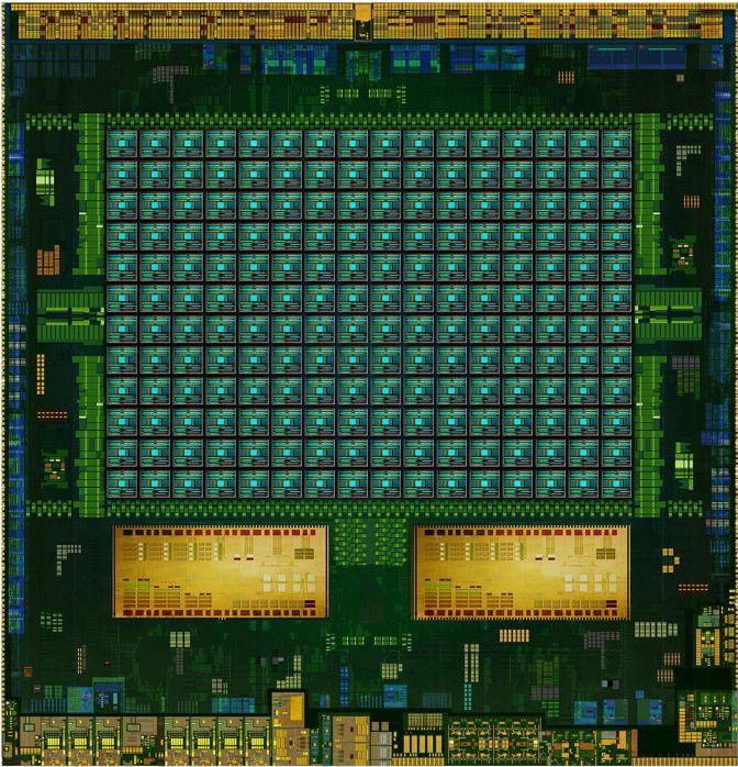
K1-64 Die Shot Mock-up (NVIDIA)
Denver comes at an interesting time for NVIDIA and for the ARM SoC industry as a whole. Apple’s unexpected launch of the ARMv8 capable Cyclone core in 2013 beat competing high-performance ARMv8 designs by nearly a year. And overall Apple set a very high bar for performance and power efficiency that is not easily matched and has greatly impacted the development and deployment schedules of other ARMv8 SoCs. At the same time because Cyclone and its derivatives are limited to iOS devices, the high-performance Android market is currently served by a mix of ARMv7 designs (A15, Krait, etc) and the just recently arrived A57 and Denver CPUs.
Showcasing the full scope of the ARM architecture license and how many different designs can execute the same instruction set, none of these ARMv8 CPUs are all that much alike. Thanks to its wide and conservatively clocked design, Apple’s Cyclone ends up looking a lot like what a recent Intel Core processor would look like if it were executing ARM instead of x86. Meanwhile ARM’s A57 design is (for lack of a better term) very ARMy, following ARM’s own power efficient design traditions and further iterating on ARM’s big.LITTLE philosophy to pair up high performance A57 and moderate performance A53 cores to allow a SoC to cover a wide power/performance curve. And finally we have Denver, perhaps the most interesting and certainly least conventional design, forgoing the established norms of Out of Order Execution (OoOE) in favor of a very wide in-order design backed by an ambitious binary translation and optimization scheme.
Counting Cores: Why Denver?
To understand Denver it’s best to start with the state of the ARM device market, and NVIDIA’s goals in designing their own CPU core. In the ARM SoC space, much has been made of core counts, both as a marketing vehicle and of value to overall performance. Much like the PC space a decade prior, when multi-core processors became viable they were of an almost immediate benefit. Even if individual applications couldn’t yet make use of multiple cores, having a second core meant that applications and OSes were no longer time-sharing a single core, which came with its own performance benefits. The OS could do its work in the background without interrupting applications as much, and greedy applications didn’t need to fight with the OS or other applications for basic resources.
However also like the PC space, the benefits of additional cores began to taper off with each additional core. One could still benefit from 4 cores over 2 cores, but unless software was capable of putting 3-4 cores to very good use, generally one would find that performance didn’t scale well with the cores. Compounding matters in the mobile ecosystem, the vast majority of devices run apps in a “monolithic” fashion with only one app active and interacting with the user at any given point in time. This meant that in absence of apps that could use 3-4 cores, there weren’t nearly as many situations in which multitasking could be employed to find work for the additional cores. The end result has been that it has been difficult for mobile devices to consistently saturate an SoC with more than a couple of cores.
Meanwhile the Cortex family of designs coming from ARM have generally allowed high core counts. Cortex-A7 is absolutely tiny, and even the more comparable Cortex-A15 isn’t all that big on the 28nm process. Quad core A15 designs quickly came along, setting the stage for the high core count situations we previously discussed.
This brings us to NVIDIA’s goals with Denver. In part due to the issues feeding 4 cores, NVIDIA has opted for a greater focus on single-threaded performance than the ARM Cortex designs they used previously. Believing that fewer, faster cores will deliver better real-world performance and better power consumption, NVIDIA set out to build a bigger, wider CPU that would do just that. The result of this project was what NVIDIA awkwardly calls their first “super core,” Denver.
Though NVIDIA wouldn’t know it at the time it was announced in 2011, Denver in 2015 is in good company that helps to prove that NVIDIA was right to focus on single-threaded performance over additional cores. Apple’s Cyclone designs have followed a very similar philosophy and the SoCs utilizing them remain the SoCs to beat, delivering chart-topping performance even with only 2 or 3 CPU cores. Deliver something similar in performance to Cyclone in the Android market and prove the performance and power benefits of 2 larger cores over 4 weaker cores, and NVIDIA would be well set in the high-end SoC marketplace.
Performance considerations aside, for NVIDIA there are additional benefits to rolling their own CPU core. First and foremost is that it reduces their royalty rate to ARM; ARM still gets a cut as part of their ISA license, but that cut is less than if you are also using ARM licensed cores. The catch of course is that NVIDIA needs to sell enough SoCs in the long run to pay for the substantial costs of developing a CPU, which means that along with the usual technical risks, there are some financial risks as well for developing your own CPU.
The second benefit to NVIDIA then is differentiation in a crowded SoC market. The SoC market has continued to shed players over the years, with players such as Texas Instruments and ST-Ericsson getting squeezed out of the market. With so many vendors using the same Cortex CPU designs, from a performance perspective their SoCs are similarly replaceable, making the risk of being the next TI all the greater. Developing your own CPU is not without risks as well – especially if it ends up underperforming the competition – but played right it means being able to offer a product with a unique feature that helps the SoC stand out from the crowd.
Finally, at the time NVIDIA announced Denver, NVIDIA also had plans to use Denver to break into the server space. With their Tesla HPC products traditionally paired x86 CPUs, NVIDIA could never have complete control over the platform, or the greater share of revenue that would entail. Denver in turn would allow NVIDIA to offer their own CPU, capturing that market and being able to play off of the synergy of providing both the CPU and GPU. Since then however the OpenPOWER consortium happened, opening up IBM’s POWER CPU lineup to companies such as NVIDIA and allowing them to add features such as NVLink to POWER CPUs. In light of that, while NVIDIA has never officially written off Denver’s server ambitions, it seems likely that POWER has supplanted Denver as NVIDIA’s server CPU of choice.
Designing Denver
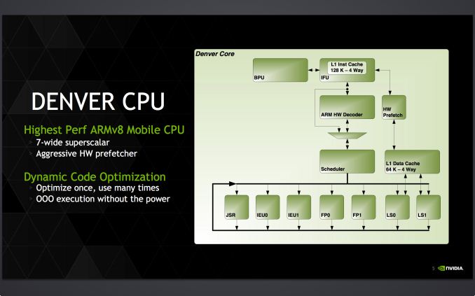
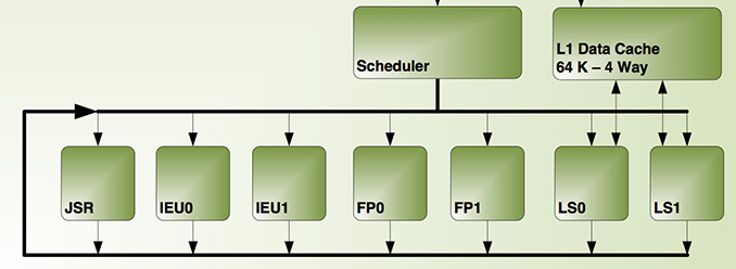
Diving into the depths of Denver, Denver is in a lot of ways exactly the kind of CPU you’d expect a GPU company to build. NVIDIA’s traditional engineering specialty is in building wide arrays of simple in-order processors, a scheme that maps well to the ridiculously parallel nature of graphics. Whether intentional to tap their existing expertise or just a result of their plan to go in such a divergent route from “traditional” CPUs, Denver makes you stop and ponder GPUs for a moment when looking at its execution workflow.
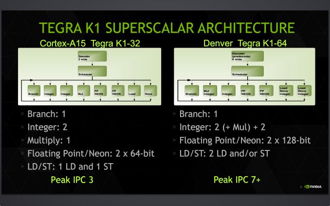
The results of NVIDIA’s labors in designing Denver has been a wide but in-order processor. With the potential to retire up to 7 operations per cycle, Denver measured front-to-back is wider than A15/A57 and wider than Cyclone. Officially NVIDIA calls this a “7+” IPC architecture, alluding to Denver’s binary translation and code optimization step, and the potential to merge operations as part of the process.
Meanwhile the existence of this code optimizer is the first sign we see that Denver is not a traditional CPU by the standards of ARM/Apple or Intel/AMD. To understand why that is we must first discuss Out of Order Execution (OoOE), why it exists, and why Denver doesn’t have it.
In traditional CPU designs, we make a distinction between in-order designs and out-of-order designs. As appropriately named, in-order designs will execute instructions in the order they receive them, and meanwhile out-of-order designs have the ability to rearrange instructions within a limited window, so long as the altered order doesn’t change the results. For the kinds of tasks that CPUs work with, OoOE improves throughput, but it does come at a cost.
Overall OoOE is considered the next logical step after in-order execution has reached its natural limits. Superscalar in-order execution can potentially scale up to a few instructions at once, but actually achieving that is rare, even with the help of good compilers. At some point other constraints such as memory accesses prevent an instruction from executing, holding up the entire program. In practice once you need performance exceeding a traditional in-order design, then you switch to out-of-order. With OoOE then it becomes possible to scale performance out further, with the ability to use the reodering process to fill wider processors and to keep from losing performance due to stalls.

K1-64 Die Shot Mock-up (NVIDIA)
The cost of OoOE is complexity, die size, and power consumption. The engines to enable OoOE can be quite large, being tasked with queuing instructions, identifying which instructions can be reordered, and ensuring instructions are safe to execute out-of-order. Similarly, there is a power cost to these engines, and that means adding OoOE to a processor can make it much larger and more power hungry, even without actually adding further units for the OoOE engines to fill. Make no mistake, the benefits of OoOE are quite large, but then so is the cost of implementing it.
As such, while OoOE has been treated as the next step after in-order processors it is not the only solution to the problem being pursued. The fundamental problems in-order processors face are a combination of hardware and software; hardware issues such as memory stalls, and software issues such as poor instruction ordering. It stands to reason then that if the performance scaling problem can be solved in hardware with OoOE, then can it be solved in software as well? It’s this school of thought that NVIDIA is pursuing in Denver.
Perhaps the critical point in understanding Denver then is that it is non-traditional for a high-performance CPU due to its lack of OoOE hardware, and for that reason it’s a CPU unlike any of its contemporaries. We’ll get back to the software aspects of Denver in a bit, but for now it’s enough to understand why NVIDIA has not pursued an OoOE design and what they have pursued instead.
Denver’s Deep Details
Due to NVIDIA’s choice not to pursue OoOE on Denver and simultaneously pursue a large, high performance core, Denver is by consumer standards a very wide CPU. With no OoOE hardware NVIDIA has been able to fill out Denver with execution units, with 7 slots’ worth of execution units backed by a native decoder wide enough to feed all of those units at once. The native decoder in particular is quite notable here, as most other CPU designs have narrower decoders that put a lower limit on their theoretical IPC. The Cortex-A15 cores in Tegra K1-32 for example only feature 3-wide decoders, despite having many more slots’ worth of execution units. Consequently a large decoder not only opens up the ability to increase IPC, but it is a sign that the CPU developer believes that their design is capable of keeping that many execution units busy enough to justify the cost of the wider decoder.
| NVIDIA CPU Core Comparison | ||||||
| K1-32 | K1-64 | |||||
| CPU | Cortex-A15 | NVIDIA Denver | ||||
| ARM ISA | ARMv7 (32-bit) | ARMv8 (32/64-bit) | ||||
| Issue Width | 3 micro-ops | 2 (ARM) or 7 (Native) micro-ops | ||||
| Pipeline Length | 18 stages | 15 stages | ||||
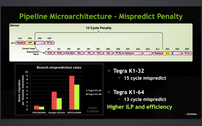
| Branch Mispredict Penalty | 15 cycles | 13 cycles | ||||
| Integer ALUs | 2 | 4 | ||||
| Load/Store Units | 1 + 1 (Dedicated L/S) | 2 (Shared L/S) | ||||
| Branch Units | 1 | 1 | ||||
| FP/NEON ALUs | 2x64-bit | 2x128-bit | ||||
| L1 Cache | 32KB I$ + 32KB D$ | 128KB I$ + 64KB D$ | ||||
| L2 Cache | 2MB | 2MB | ||||
These execution units themselves are fairly unremarkable, but none the less are very much at the heart of Denver. Compared again to Terga 4, there are twice as many load/store units, and the NEON units have been extended from 64-bits wide to 128-bits wide, allowing them to retire up to twice as much work per cycle if they can be completely filled.
Internally Denver executes instructions using the Very Long Instruction Word (VLIW) format, which is an instruction format that these days is more common with GPUs than it is CPUs, making it another vaguely GPU-like aspect of Denver. In VLIW all instructions are packed into a single word and sent through the pipeline at once, rather than handing each slot its own instruction. Each VLIW instruction is variable in length, and in turn the length of the operation is similarly variable, depending in part on factors such as the number of registers any given instruction operates upon. With a maximum VLIW instruction size of 32 bytes, this means that the number of operations a single instruction can contain is dependent on the operations, and it’s possible for large operations to fill out the VLIW early.
Another one of Denver’s unusual aspects is its internal instruction format, which is very different from ARMv7 or ARMv8. Though the specific format is beyond the scope of this article, it has long been rumored that Denver was originally meant to be an x86 design, with Denver’s underlying design and binary translation pairing intended to allow for an x86 implementation without infringing on any x86 hardware patents. Whether that is true or not, the end result of Denver is that owing to NVIDIA’s decision to solve their needs in software, NVIDIA was able to create an architecture whose design is decoupled from the actual instruction set it is executing.
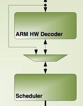
Yet in spite of this architectural choice, Denver still needs to be able to execute ARM code as well as native code from binary translation, which leads to one more interesting wrinkle to Denver’s design. Denver has not one but two decoders, the native decoder and a proper ARM decoder. Designed to work in situations where Denver’s software optimizer is not worth running or can’t translate in time – such as with brand new code segments – the ARM decoder allows for Denver to directly decode ARM instructions.
The ARM decoder is not quite a backup, but it is not intended to be the main source of operations for Denver over the long run. Rather the bulk of the work for Denver should come from its binary translator, and only a small fraction of infrequently used code should hit the ARM decoder. At only 2 instructions wide this decoder is narrower than even A15’s decoder, not to mention it forms an entirely in-order pipeline that misses out on the instruction rescheduling and other optimizing benefits of the software code optimizer. Never the less it serves an important role in situations where Denver can’t use native code by giving it a means to immediately begin executing ARM code. This as a result makes Denver a kind of hybrid design, capable of executing either ARM instructions or NVIDIA’s own internal microcode.
Meanwhile Denver’s overall pipeline stands at 15 stages deep. Despite the overall width of Denver this actually makes the pipeline shorter than the 18 stage A15 by a few stages. And similarly, the penalty for branch mispredictions is down from 15 cycles in A15 to 13 cycles in Denver.
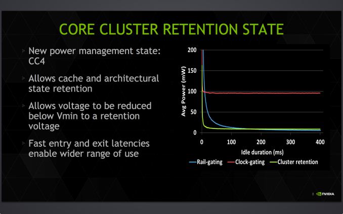
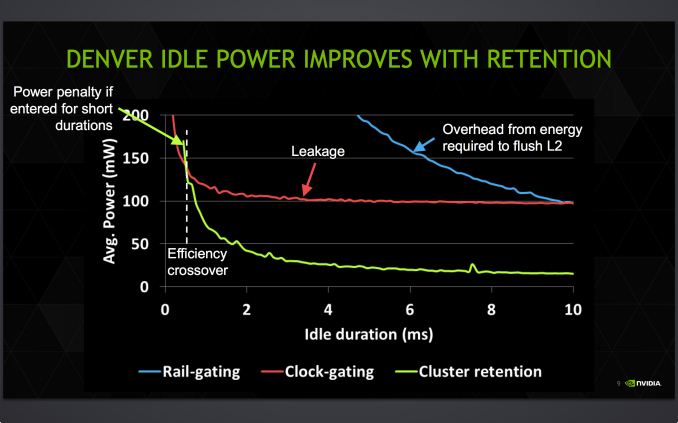
Last but not least, on the logical level NVIDIA has also been working to further reduce their power consumption through a new mode called CC4. CC4 is essentially a deeper state of sleep that’s not quite power-gating the entire CPU, but none the less results in most of the CPU being shut off. What ends up being retained in CC4 is the cache and what NVIDIA dubs the “architectural state” of the processor, a minimal set of hardware that allows the core voltage to drop below traditional Vmin and instead hold at just enough voltage to retain the contents of the cache and state, as no work needs to be done in this state. It's worth noting that we've seen similar power collapse states as far back as the A15 though, so the idea isn't necessarily new.
CC4 as a result is intended to be a relatively fast sleep state given its depth, with Denver able to enter and exit it faster than power-gating, and consequently it can be used more frequently. That said since it is deeper than other sleep states it is also slower than them, meaning the CPUIdle governor needs to take this into account and only select CC4 when there’s enough time to take advantage of it. Otherwise if Denver enters CC4 and has to come out of it too soon, the processor can end up wasting more power setting up CC4 than a very short CC4 duration would save.
Of course CC4 is just one of many factors in Denver’s power consumption. Hardware and software alike plays a role, from the silicon itself and the leakage characteristics of the physical transistors to the binary translation layer necessary for Denver to operate at its peak. And that brings us to the final and more crucial piece of the Denver puzzle: the binary translation layer.
The Secret of Denver: Binary Translation & Code Optimization
As we alluded to earlier, NVIDIA’s decision to forgo a traditional out-of-order design for Denver means that much of Denver’s potential is contained in its software rather than its hardware. The underlying chip itself, though by no means simple, is at its core a very large in-order processor. So it falls to the software stack to make Denver sing.
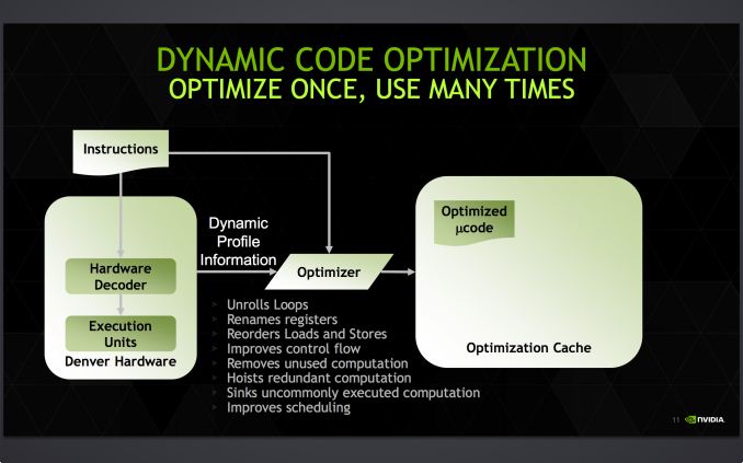
Accomplishing this task is NVIDIA’s dynamic code optimizer (DCO). The purpose of the DCO is to accomplish two tasks: to translate ARM code to Denver’s native format, and to optimize this code to make it run better on Denver. With no out-of-order hardware on Denver, it is the DCO’s task to find instruction level parallelism within a thread to fill Denver’s many execution units, and to reorder instructions around potential stalls, something that is no simple task.
Starting first with the binary translation aspects of DCO, the binary translator is not used for all code. All code goes through the ARM decoder units at least once before, and only after Denver realizes it has run the same code segments enough times does that code get kicked to the translator. Running code translation and optimization is itself a software task, and as a result this task requires a certain amount of real time, CPU time, and power. This means that it only makes sense to send code out for translation and optimization if it’s recurring, even if taking the ARM decoder path fails to exploit much in the way of Denver’s capabilities.
This sets up some very clear best and worst case scenarios for Denver. In the best case scenario Denver is entirely running code that has already been through the DCO, meaning it’s being fed the best code possible and isn’t having to run suboptimal code from the ARM decoder or spending resources invoking the optimizer. On the other hand then, the worst case scenario for Denver is whenever code doesn’t recur. Non-recurring code means that the optimizer is never getting used because that code is never seen again, and invoking the DCO would be pointless as the benefits of optimizing the code are outweighed by the costs of that optimization.
Assuming that a code segment recurs enough to justify translation, it is then kicked over to the DCO to receive translation and optimization. Because this itself is a software process, the DCO is a critical component due to both the code it generates and the code it itself is built from. The DCO needs to be highly tuned so that Denver isn’t spending more resources than it needs to in order to run the DCO, and it needs to produce highly optimal code for Denver to ensure the chip achieves maximum performance. This becomes a very interesting balancing act for NVIDIA, as a longer examination of code segments could potentially produce even better code, but it would increase the costs of running the DCO.
In the optimization step NVIDIA undertakes a number of actions to improve code performance. This includes out-of-order optimizations such as instruction and load/store reordering, along register renaming. However the DCO also behaves as a traditional compiler would, undertaking actions such as unrolling loops and eliminating redundant/dead code that never gets executed. For NVIDIA this optimization step is the most critical aspect of Denver, as its performance will live and die by the DCO.
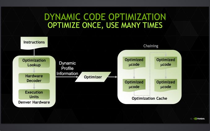
Denver's optimization cache: optimized code can call other optimized code for even better performance
Once code leaves the DCO, it is then stored for future use in an area NVIDIA calls the optimization cache. The cache is a 128MB segment of main memory reserved to hold these translated and optimized code segments for future reuse, with Denver banking on its ability to reuse code to achieve its peak performance. The presence of the optimization cache does mean that Denver suffers a slight memory capacity penalty compared to other SoCs, which in the case of the N9 means that 1/16th (6%) of the N9’s memory is reserved for the cache. Meanwhile, also resident here is the DCO code itself, which is shipped and stored as already-optimized code so that it can achieve its full performance right off the bat.
Overall the DCO ends up being interesting for a number of reasons, not the least of which are the tradeoffs are made by its inclusion. The DCO instruction window is larger than any comparable OoOE engine, meaning NVIDIA can look at larger code blocks than hardware OoOE reorder engines and potentially extract even better ILP and other optimizations from the code. On the other hand the DCO can only work on code in advance, denying it the ability to see and work on code in real-time as it’s executing like a hardware out-of-order implementation. In such cases, even with a smaller window to work with a hardware OoOE implementation could produce better results, particularly in avoiding memory stalls.
As Denver lives and dies by its optimizer, it puts NVIDIA in an interesting position once again owing to their GPU heritage. Much of the above is true for GPUs as well as it is Denver, and while it’s by no means a perfect overlap it does mean that NVIDIA comes into this with a great deal of experience in optimizing code for an in-order processor. NVIDIA faces a major uphill battle here – hardware OoOE has proven itself reliable time and time again, especially compared to projects banking on superior compilers – so having that compiler background is incredibly important for NVIDIA.
In the meantime because NVIDIA relies on a software optimizer, Denver’s code optimization routine itself has one last advantage over hardware: upgradability. NVIDIA retains the ability to upgrade the DCO itself, potentially deploying new versions of the DCO farther down the line if improvements are made. In principle a DCO upgrade not a feature you want to find yourself needing to use – ideally Denver’s optimizer would be perfect from the start – but it’s none the less a good feature to have for the imperfect real world.
Case in point, we have encountered a floating point bug in Denver that has been traced back to the DCO, which under exceptional workloads causes Denver to overflow an internal register and trigger an SoC reset. Though this bug doesn’t lead to reliability problems in real world usage, it’s exactly the kind of issue that makes DCO updates valuable for NVIDIA as it gives them an opportunity to fix the bug. However at the same time NVIDIA has yet to take advantage of this opportunity, and as of the latest version of Android for the Nexus 9 it seems that this issue still occurs. So it remains to be seen if BSP updates will include DCO updates to improve performance and remove such bugs.
SPECing Denver's Performance
Finally, before diving into our look at Denver in the real world on the Nexus 9, let’s take a look at a few performance considerations.
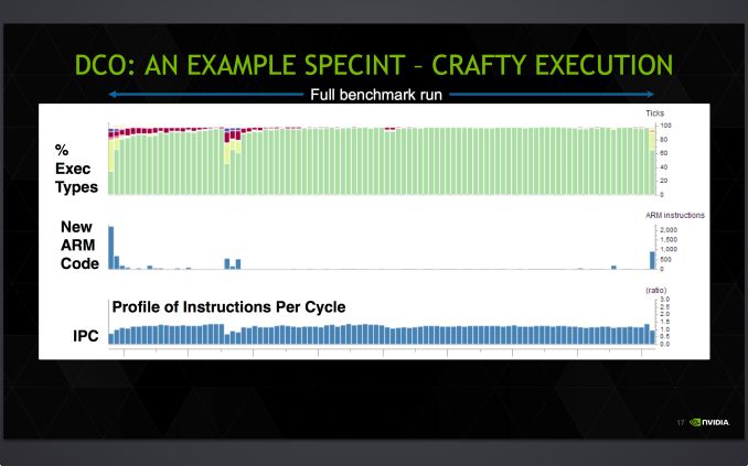
With so much of Denver’s performance riding on the DCO, starting with the DCO we have a slide from NVIDIA profiling the execution of SPECInt2000 on Denver. In it NVIDIA showcases how much time Denver spends on each type of code execution – native ARM code, the optimizer, and finally optimized code – along with an idea of the IPC they achieve on this benchmark.
What we find is that as expected, it takes a bit of time for Denver’s DCO to kick in and produce optimized native code. At the start of the benchmark execution with little optimized code to work with, Denver initially executes ARM code via its ARM decoder, taking a bit of time to find recurring code. Once it finds that recurring code Denver’s DCO kicks in – taking up CPU time itself – as the DCO begins replacing recurring code segments with optimized, native code.
In this case the amount of CPU time spent on the DCO is never too great of a percentage of time, however NVIDIA’s example has the DCO noticeably running for quite some time before it finally settles down to an imperceptible fraction of time. Initially a much larger fraction of the time is spent executing ARM code on Denver due to the time it takes for the optimizer to find recurring code and optimize it. Similarly, another spike in ARM code is found roughly mid-run, when Denver encounters new code segments that it needs to execute as ARM code before optimizing it and replacing it with native code.
Meanwhile there’s a clear hit to IPC whenever Denver is executing ARM code, with Denver’s IPC dropping below 1.0 whenever it’s executing large amounts of such code. This in a nutshell is why Denver’s DCO is so important and why Denver needs recurring code, as it’s going to achieve its best results with code it can optimize and then frequently re-use those results.
Also of note though, Denver’s IPC per slice of time never gets above 2.0, even with full optimization and significant code recurrence in effect. The specific IPC of any program is going to depend on the nature of the code, but this serves as a good example of the fact that even with a bag full of tricks in the DCO, Denver is not going to sustain anything near its theoretical maximum IPC of 7. Individual VLIW instructions may hit 7, but over any period of time if a lack of ILP in the code itself doesn’t become the bottleneck, then other issues such as VLIW density limits, cache flushes, and unavoidable memory stalls will. The important question is ultimately whether Denver’s IPC is enough of an improvement over Cortex A15/A57 to justify both the power consumption costs and the die space costs of its very wide design.
NVIDIA's example also neatly highlights the fact that due to Denver’s favoritism for code reuse, it is in a position to do very well in certain types of benchmarks. CPU benchmarks in particular are known for their extended runs of similar code to let the CPU settle and get a better sustained measurement of CPU performance, all of which plays into Denver’s hands. Which is not to say that it can’t also do well in real-world code, but in these specific situations Denver is well set to be a benchmark behemoth.
To that end, we have also run our standard copy of SPECInt2000 to profile Denver’s performance.
| SPECint2000 - Estimated Scores | ||||||
| K1-32 (A15) | K1-64 (Denver) | % Advantage | ||||
| 164.gzip |
869
|
1269
|
46%
|
|||
| 175.vpr |
909
|
1312
|
44%
|
|||
| 176.gcc |
1617
|
1884
|
17%
|
|||
| 181.mcf |
1304
|
1746
|
34%
|
|||
| 186.crafty |
1030
|
1470
|
43%
|
|||
| 197.parser |
909
|
1192
|
31%
|
|||
| 252.eon |
1940
|
2342
|
20%
|
|||
| 253.perlbmk |
1395
|
1818
|
30%
|
|||
| 254.gap |
1486
|
1844
|
24%
|
|||
| 255.vortex |
1535
|
2567
|
67%
|
|||
| 256.bzip2 |
1119
|
1468
|
31%
|
|||
| 300.twolf |
1339
|
1785
|
33%
|
|||
Given Denver’s obvious affinity for benchmarks such as SPEC we won’t dwell on the results too much here. But the results do show that Denver is a very strong CPU under SPEC, and by extension under conditions where it can take advantage of significant code reuse. Similarly, because these benchmarks aren’t heavily threaded, they’re all the happier with any improvements in single-threaded performance that Denver can offer.
Coming from the K1-32 and its Cortex-A15 CPU to K1-64 and its Denver CPU, the actual gains are unsurprisingly dependent on the benchmark. The worst case scenario of 176.gcc still has Denver ahead by 17%, meanwhile the best case scenario of 255.vortex finds that Denver bests A15 by 67%, coming closer than one would expect towards doubling A15's performance entirely. The best case scenario is of course unlikely to occur in real code, though I’m not sure the same can be said for the worst case scenario. At the same time we find that there aren’t any performance regressions, which is a good start for Denver.
If nothing else it's clear that Denver is a benchmark monster. Now let's see what it can do in the real world.
CPU Performance
While Denver’s architecture is something fascinating to study, it’s important to see how well this translates to the real world. Denver on paper is a beast, but in the real world there are a number of factors to consider, not the least of which is the effectiveness of NVIDIA’s DCO. We’ve laid out that Denver’s best and worst case scenarios heavily ride on the DCO, and for NVIDIA to achieve their best-case performance they need to be able to generate and feed Denver with lots and lots of well optimized code. If Denver spends too much time working directly off of ARM code or can’t do a good job optimizing the recurring code it finds then Denver will struggle. Meanwhile other important factors are in play as well, including the benefits and drawbacks of Denver’s two cores versus competing SoC’s quad A15/A57 configurations, and in thermally constrained scenarios Denver’s ability to deliver good performance while keeping its power consumption in check.
In order to test this and general system performance, we turn our suite of benchmarks that include browser performance tests, general system tests, and game-type benchmarks. As Denver relies on code-morphing to enable out of order execution and speculative execution, most of these benchmarks should be able to show ideal performance as loop performance in Denver is basically second to none. While most of these benchmarks are showing their age, they should be usable for valid comparisons until we move to our new test suite.
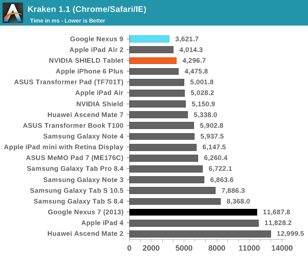
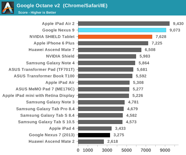
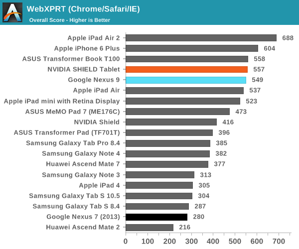
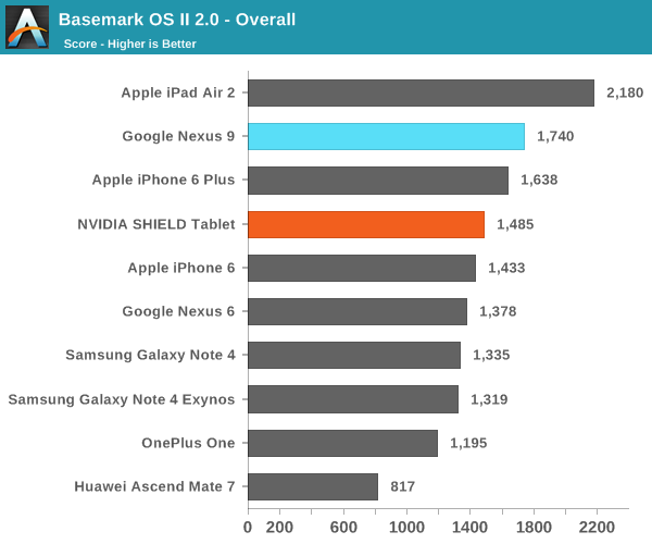
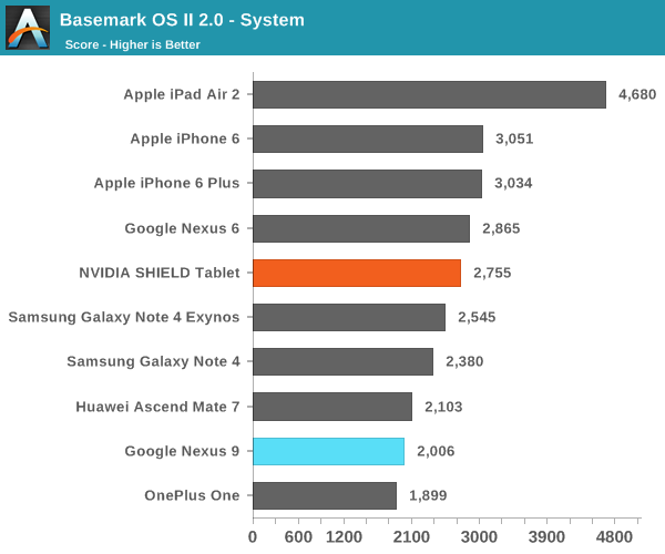
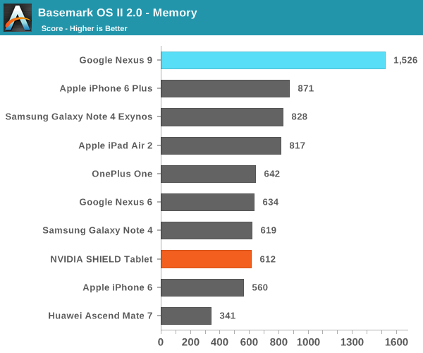
The Basemark System test seems to contribute quite strongly to how the Nexus 9 performs in the overall subtest. Given that this is a storage performance benchmark, it's likely that Basemark OS II has issues similar to Androbench on 5.0 Lollipop or that random I/O is heavily prioritized in this test.
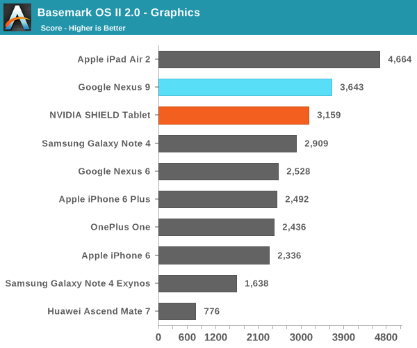
There's a noticeable performance uplift in the graphics test, and although not exactly part of the CPU this does seem at least somewhat plausible as GPU driver updates can improve performance over time.
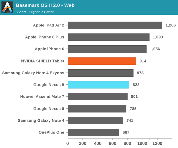
Overall, performance seems to be quite checkered, although improved from our initial evaluation of the Nexus 9. Unfortunately, even in benchmarks where the DCO should be able to easily unroll loops to achieve massive amounts of performance, we see inconsistent performance in Denver. This may come down to an issue with the DCO, or even more simply the fact that Denver is spending more time than it would like to directly executing ARM code as opposed to going through the DCO.
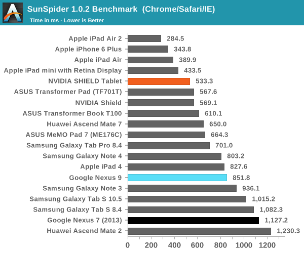
In this case looking at the SunSpider and Kraken javascript benchmarks offers an interesting proxy case for exactly that scenario. SunSpider on modern CPUs executes extremely quickly, so quickly that the individual tests are often over in only a couple of dozen of milliseconds. This is a particularly rough scenario for Denver, as it doesn’t provide Denver with much time to optimize, even if the code is run multiple times. Meanwhile Kraken pushes many similar buttons, but its tests are longer, and that gives Denver more time to optimize. Consequently we find that Denver’s SunSpider performance is quite poor – underperforming even the A15-based Tegra K1-32 – while Denver passes even the iPad Air 2 in Kraken.
Ultimately this kind of inconsistent performance is a risk and a challenge for Denver. While no single SoC tops every last CPU benchmark, we also don’t typically see the kind of large variations that are occurring with Denver. If Denver’s lows are too low, then it definitely impacts the suitability of the SoC for high-end devices, as users have come to expect peppy performance at all times.
In practice, I didn't really notice any issues with the Nexus 9's performance, although there were odd moments during intense multitasking where I experienced extended pauses/freezes that were likely due to the DCO getting stuck somewhere in execution, seeing as how the DCO can often have unexpected bugs such as repeated FP64 multiplication causing crashes. In general, I noticed that the device tended to also get hot even on relatively simple tasks, which doesn't bode well for battery life. This is localized to the top of the tablet, which should help with user comfort although this comes at the cost of worse sustained performance.
GPU Performance
While Denver is new, the Kepler GPU in the Tegra K1 is mostly a known quantity by now. In the Nexus 9, the GPU is still a single SMX clocked to 852 MHz. In order to verify performance, we turn to our standard test suite. For the most part, our GPU-bound tests are meant to represent gaming performance although tests like 3DMark can have CPU-bound aspects while GFXBench tends towards being a pure GPU test.
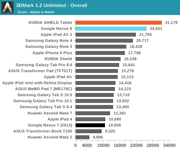
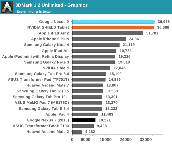
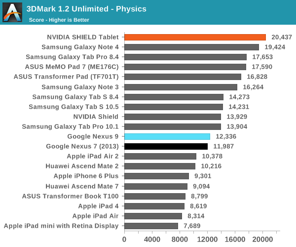
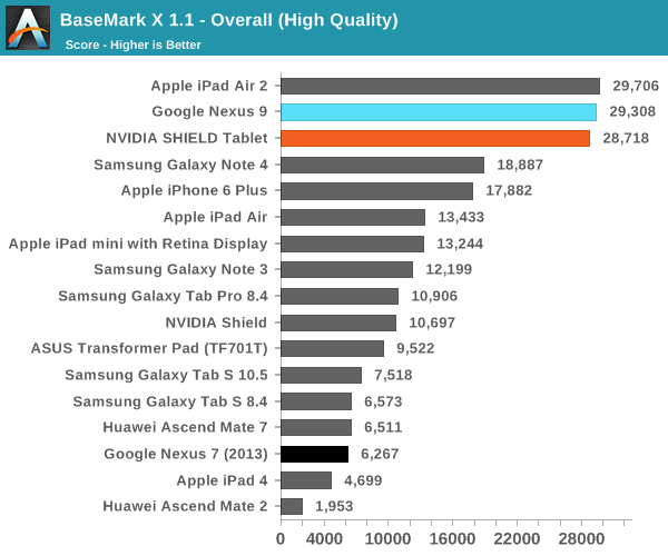
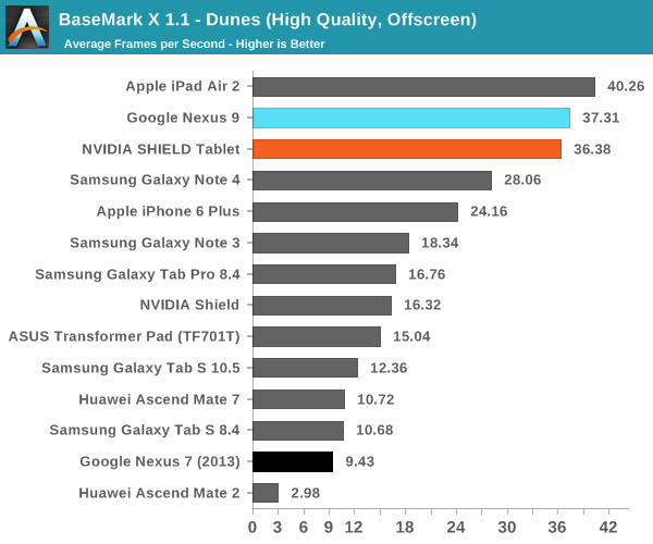
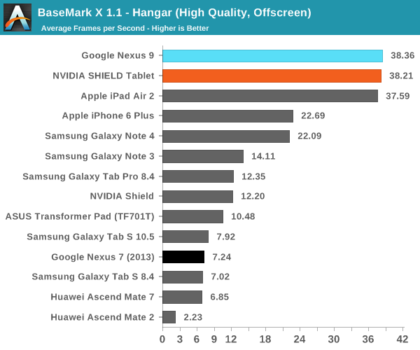
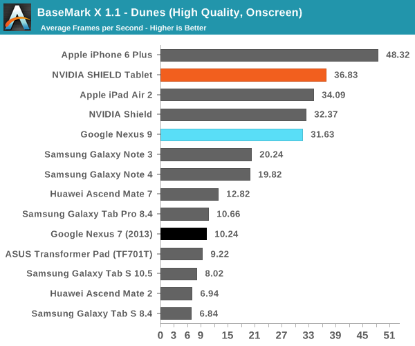
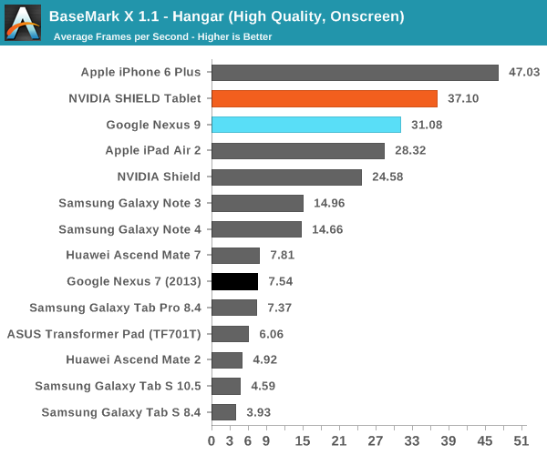
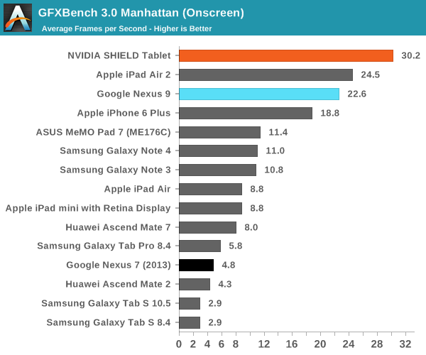
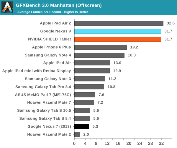
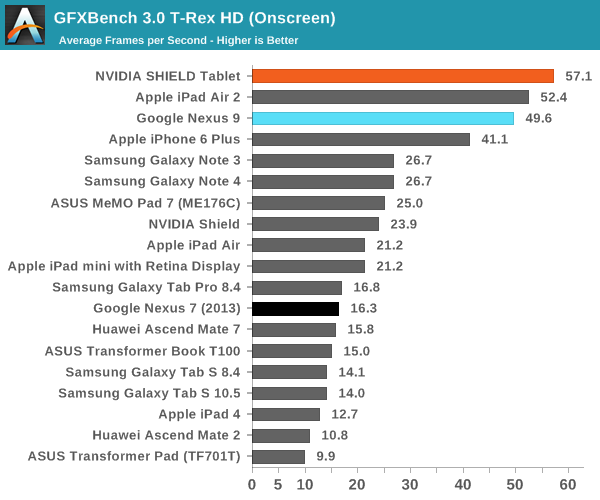
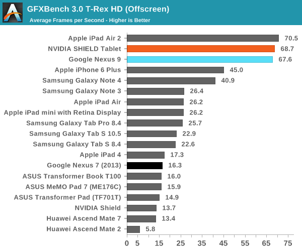
The Nexus 9's GPU has effectively identical performance to what we saw in the SHIELD Tablet, which means that the Nexus 9 should be able to support a broad range of games without performance issues. There is a bit of a noticeable performance delta when comparing on-screen performance, but this is simply due to the higher resolution of the Nexus 9's display. The one notable exception is the 3DMark physics test, which seems to scale with core count quite well, and that causes Denver to fall slightly short of the quad A15 configuration.
NAND Performance
While storage performance can often be secondary to a smooth user experience, poor storage performance is extremely painful. This is similar to RAM, where the difference between 2 and 3 GB is generally academic, while the difference between 512MB and 1 GB is enormous. While there have been some issues with Androbench with the move to Android 5.0, it seems that the timer issues have since been resolved, so it's possible to resume using the results from Androbench to get a rough idea of NAND performance.
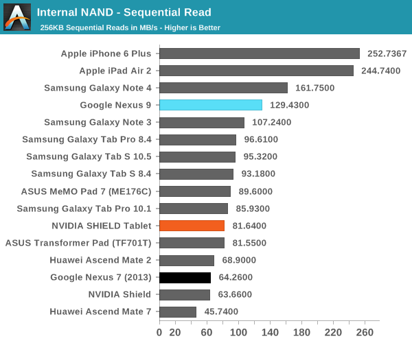
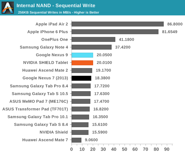
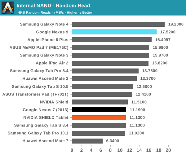
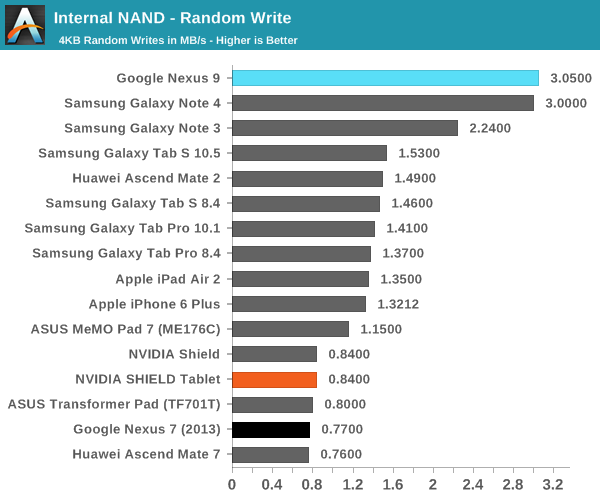
Here the Nexus 9 doesn't suffer nearly as much from full disk encryption that is forcibly enabled on the device; performance is noticeably higher than what we see in the Nexus 6. This seems to lend some credence to the theory that CPUs with ARM v8 ISA would be better suited to handling the need to encrypt and decrypt storage in real time. I tested the Nexus 9 with a custom kernel without full disk encryption to see how Androbench scores might change, but this didn't have a noticeable impact which seems to back this theory, although I'm still not confident that FDE is a good idea to enforce across all new devices.
The NAND itself, a Samsung eMMC package designated by the name BWBC3R, seems to be quite performant outside of pure sequential access, which seems to suggest that HTC hasn't skimped out in this area at all, and the use of F2FS is responsible for some of the best random I/O scores in any mobile devices we've tested thus far.
Display
For those that are uninitiated to the world of displays, a display seems relatively simple. After all, it just needs to have high resolution, pretty colors, high brightness, and high contrast. However, there’s a great deal of complexity to this issue. Even excluding the actual structure of a display, the characteristics of a display can strongly affect perception. Poor display calibration, low brightness, high reflectance, and low contrast can all affect the experience. In addition, something as simple as subpixel arrangement and the thin-film transistor design can have significant impacts on viewing angles and battery life.
In order to test these things, we use SpectraCal’s CalMAN 5 Ultimate and X-Rite’s i1pro2 spectrophotometer to ensure accuracy in our testing, in conjunction with subjective testing to get a good idea of overall display performance. As always, we target sRGB gamut and 2.2 gamma as these are the industry standard. While there are many arguments for larger gamuts and different gamma curves, the goal of our display calibration testing is to make sure that a display will be reasonably accurate in its reproduction of content as an artist intended. Without this calibration, videos, photos, and other content can appear "off".
While we still don’t have an accurate reflectance test, I spent a great deal of time wondering why the display on the Nexus 9 seemed to have more distracting glare than most. This was strange to me as the display was obviously laminated with no perceivable viewing angle degradation that comes with non-laminated displays. It seems that whatever material HTC has used to laminate the display isn’t quite ideal in this case, as at some point in the display stack there’s an obvious secondary reflection. This is an issue relating to a lower index of refraction, so it’s likely that some other characteristic was valued over reflectance.
Other than this, the only other immediately noticeable flaw is the display’s backlight bleed. To me, it’s quite obvious that the display gets lighter at the edges much like what I’ve seen on the Nexus 5. It seems that this is related to the backlight configuration, although given the high brightness of the panel I'm not sure that this can be avoided.
Before we get into the objective testing, I also wanted to mention that this display has “dual-domain pixels” similar to the iPad Air 2 and iPhone 6. The level of angling seems to be much more significant though, which seems to make the purple blacks much more obvious, but outside of this shift in black point it’s almost impossible to see shifts in color with changes in viewing angle. The microscope photo combined with some casual examination under sunlight suggests that the digitizer has been integrated into the display for improved clarity. The resolution is also quite high for a tablet, and while I can obviously pick out aliasing when closely examining the display, at a normal viewing distance I don’t really see any of these problems.
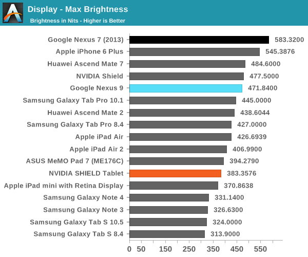
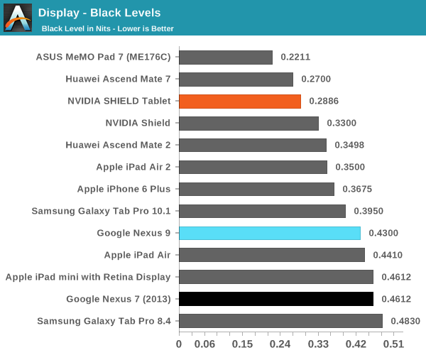
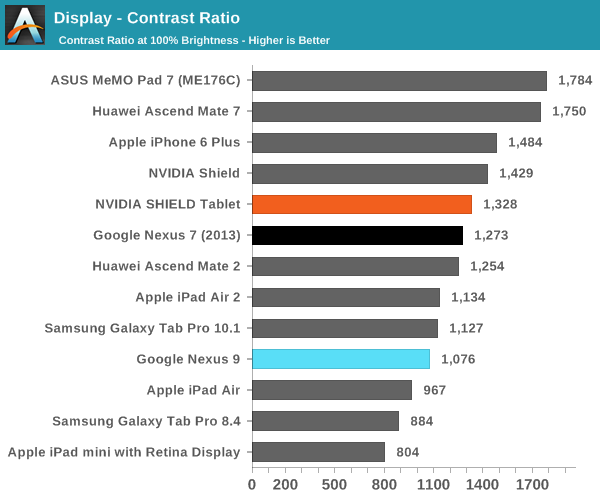
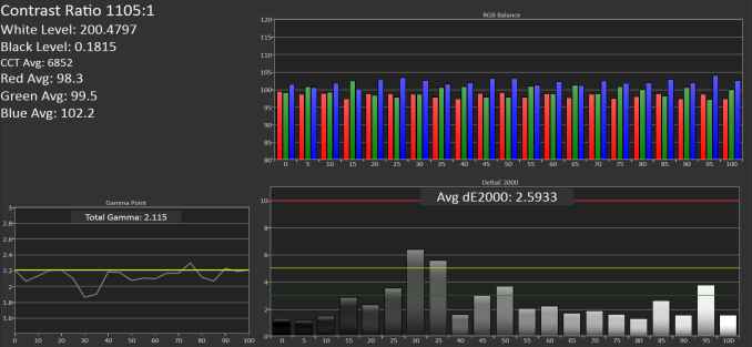
The brightness of the Nexus 9's display ends up higher than what we see with the iPad Air 2. Contrast is approximately equal to what we see in the iPad Air 2, which is good but definitely not the perfect inky blacks that one might be used to from AMOLED.
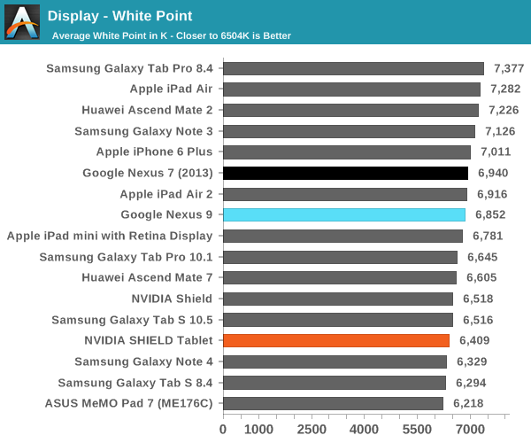
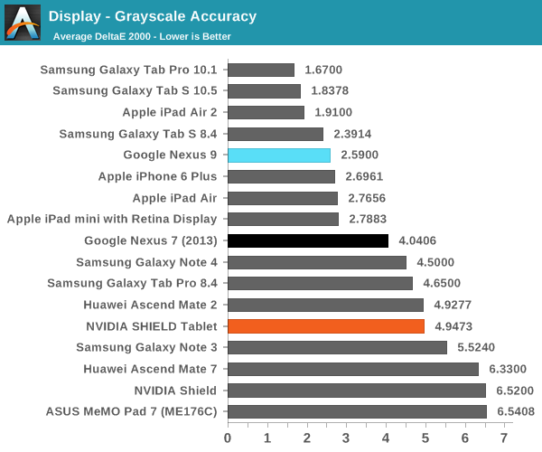
The next aspect of our display test suite is the grayscale test, which looks at the color balance and brightness of various shades of grayscale from black to white. Here, the Nexus 9 really does a great job across the board. If I were to nitpick, there is a bit of extra blue in the display but it’s really nothing worth talking about. Google does seem to consistently favor a lower contrast look when the gamma curve is dead on the mark, but on average it’s close enough to a power 2.2 curve that it doesn’t make a difference when viewing the display.
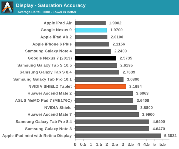
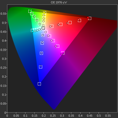
While grayscale is important, colors are really the hardest part to get right in a display. Here, the Nexus 9 does an amazing job in our saturation test. I really don’t have anything else to say here as pretty much everything is on the mark. At this point, it’s pretty clear that most Nexus devices have a strong focus on display quality, and the Nexus 9 is no exception.
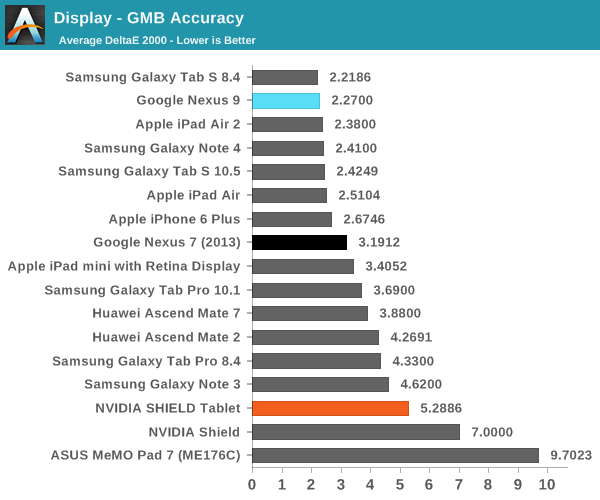
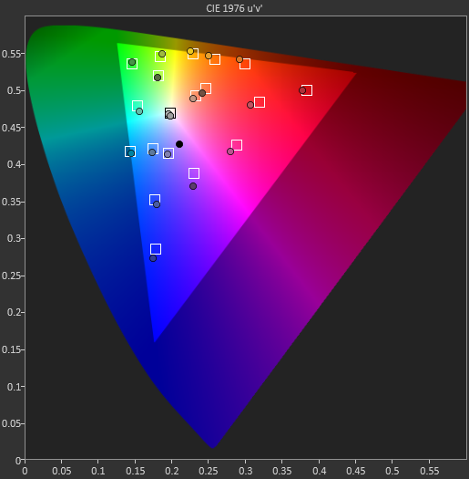
Finally, the Gretag MacBeth test shows that the Nexus 9 is quite accurate with color even outside of the basic primary and secondary colors. There shouldn’t be any issues with viewing content that has high requirements for color accuracy. Overall, the Nexus 9 display is great with only two real issues of note, namely the reflectance issue and the backlight bleed. While neither are deal-breakers, fixing these issues would make this display fall under a short list of the best mobile displays I’ve seen all year. For now, it sits just shy of that list. I definitely have to applaud Google in this case as they haven’t fallen into the trap of wider gamuts, bluer white points, dynamic contrast, and other “features” for the sake of showroom appeal.
Battery Life
It goes without saying that battery life is one of the most important aspects of a mobile device. After all, a mobile device isn’t really mobile if it can only be used for an hour before running out of battery. In order to test this, we turn to our standard suite of battery life tests, which include our web browser battery life test, along with some compute-bound benchmarks to characterize battery life across various use cases.
However, as the Nexus 9 introduces such a unique CPU architecture, I felt that it was necessary to try and adequately capture the full extent of battery life. To this end, I’ve introduced a new test that is really quite simple but important, as we can start to separate display power from everything else since it can often be the single largest consumer of power in a test. In order to do this, everything that could run during a test is disabled, and the device is placed in airplane mode with the display at 200 nits. A white image is displayed on the screen from a full charge until the device shuts down.
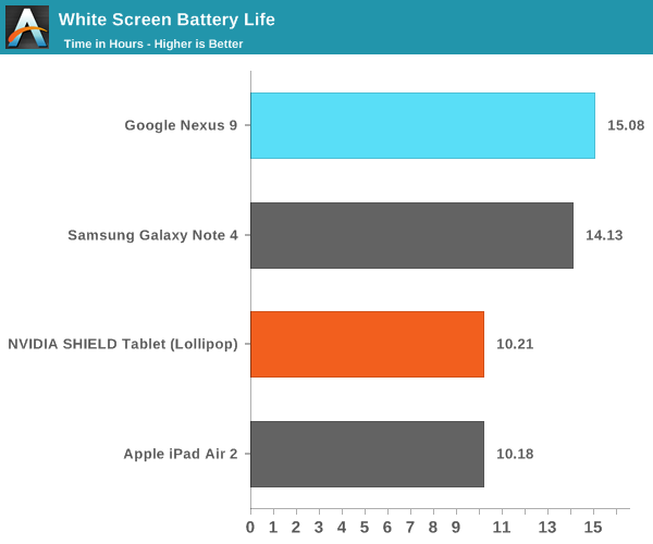
Interestingly enough, the display runtime on the Nexus 9 is about as good as it gets when compared to other devices for which we have data. I suspect we’re looking at the direct result of the large battery combined with an efficient display, as the Nexus 9 can last as long as 15 hours in this test compared to the iPad Air 2’s 10 hours.
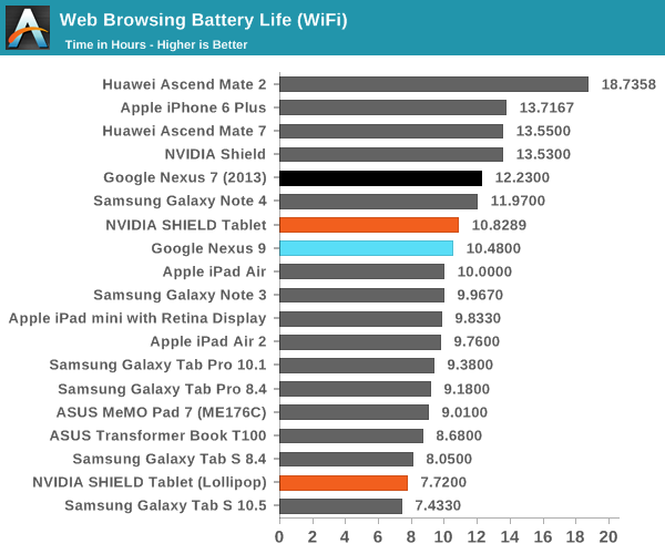
Unfortunately, the massive lead that we saw with the pure display test is significantly eroded in our web browser test. Our web test is primarily focused upon CPU, connectivity, and display efficiency. Seeing as how the Nexus 9’s display is far ahead of the iPad Air 2 and connectivity should be broadly similar in power efficiency, it seems that all of the efficiency gains from the display have gone into powering the Denver CPUs. It’s likely that process has a significant effect on this, so the more valid comparison is between SHIELD Tablet and the Nexus 9. At any rate, the Nexus 9 does manage to deliver solid battery life performance in this test which is definitely a good thing.
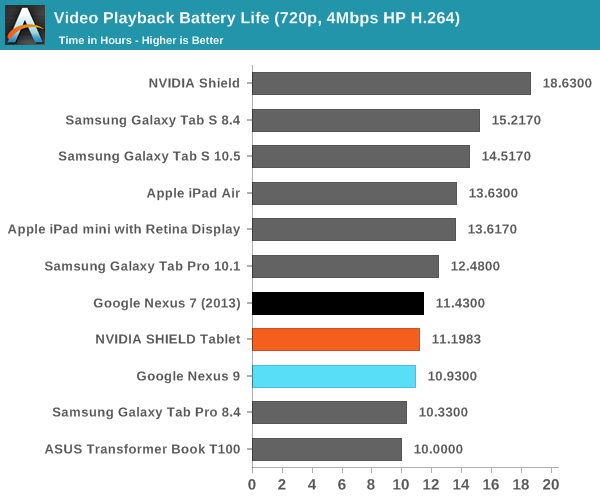
When we move to our pure video test, the Nexus 9 does have a minor regression when compared to the Nexus 7 (2013) and SHIELD Tablet. In this case, the AMOLED displays on the Galaxy Tab S line make for an easy victory due to the relatively high amount of black displayed in the content. The gap is closed between the two devices though, due to a reduced focus on SoC power.
While our web browsing test can give some idea of efficiency, there are often cases where more compute is directly used to support a better experience. To try and test for these compute-bound cases, we use Basemark OS II’s CPU battery life test and GFXBench’s T-Rex rundown for a GPU battery life test. As with the web browsing tests, these are run at 200 nits to keep things relatively equal.
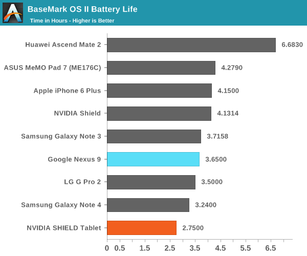
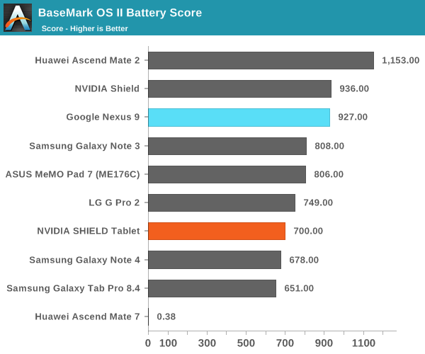
In Basemark OS II, the Nexus 9 does a surprisingly good job as the CPU manages to keep incredibly high sustained performance. The large battery and efficient display seem to help to a significant extent.
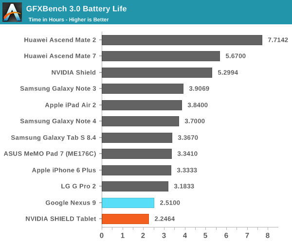
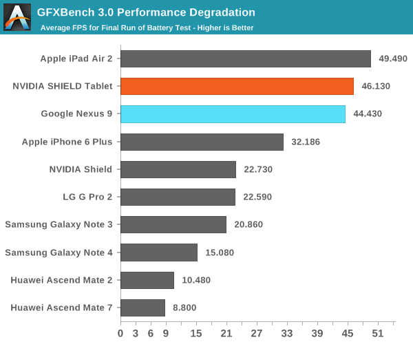
In GFXBench, it seems that not much changes overall. The GPU is definitely more power hungry than the PowerVR Series 6XT line-up and sustained performance is noticeably worse, but it’s in line with the SHIELD Tablet. End of run performance ends up a bit lower, but higher than one might expect. This is likely due to differing ambient temperatures. In practice, skin temperatures are about 45C in this test and localized to the top half of the device, and it’s likely that internal temperatures are around 80C as well. Seeing as how Tegra K1 can theoretically draw 33W in platforms such as the Jetson TK1 dev board with active cooling, it's incredibly impressive to see NVIDIA effectively keep such a powerful SoC within the constraints of a passively-cooled tablet.
Charge Time
While battery life is one part of the equation, charge time is an equally important aspect of overall battery life. To measure this, we measure the time from when charging begins to when the device reaches 100% charge. This is confirmed by taking measurements at the power outlet to make sure that power draw is below a certain level.
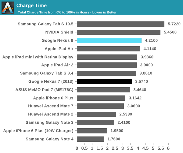
In this regard, the Nexus 9 is merely average for a tablet, although it does fall behind the competition as it uses a 5V, 1.5A charger for 7.5W instead of the 12-15W chargers that we’ve seen recently. It shouldn’t be a big issue, but in general this does mean that devices like the Galaxy Note 4 are actually better at battery life overall when compared to most tablets.
Software
With the Nexus 9, Google has released the biggest upgrade to Android since 4.0. In some ways, Android 5.0 represents one of the biggest shifts in the design of the OS ever. While we’ve had JIT compiling on Dalvik since Android 2.2, this has remained largely static for the past few years during Android’s monumental growth. With Android 5.0, we see the introduction of Android Runtime, or ART. Instead of trying to compile the application right before execution, ART does most of the compilation well before the application is launched. This incurs higher storage requirements, longer app-install times, and longer first-boot times, but with great benefits to performance. Google has done a great deal of work in general to try and resolve performance issues, as we first detailed in our coverage on ART.
While performance is one major aspect of Android 5.0, Google has also fundamentally redesigned the interface. To replace Holo, Google has introduced Material Design, which emphasizes depth, physics, animation, and a new palette of colors. While it would be great to go over all of these aspects of the Nexus 9, it’s best to refer to Brandon's review of Android 5.0 Lollipop for these issues. Instead, for this review I will mostly focus on the Lollipop experience specific to the Nexus 9. This means that the focus will be on performance of the device in general usage, along with the app ecosystem for Android tablets.
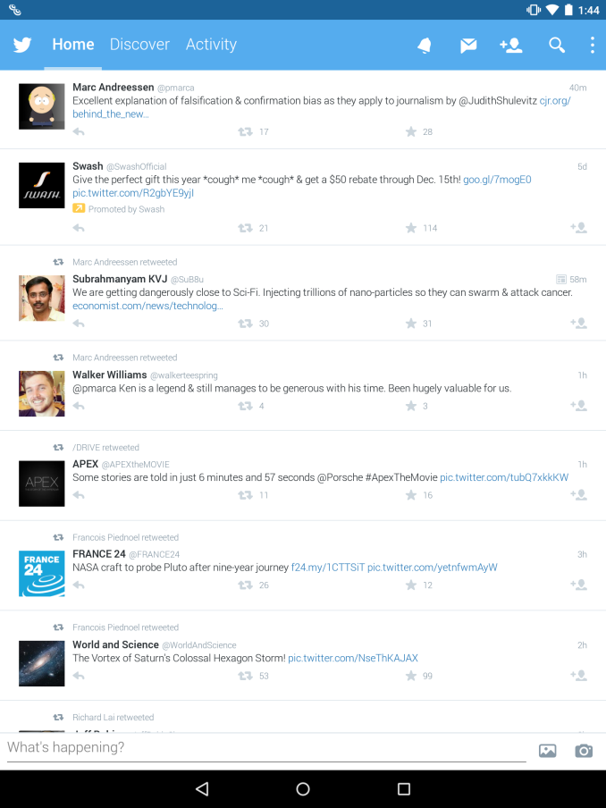
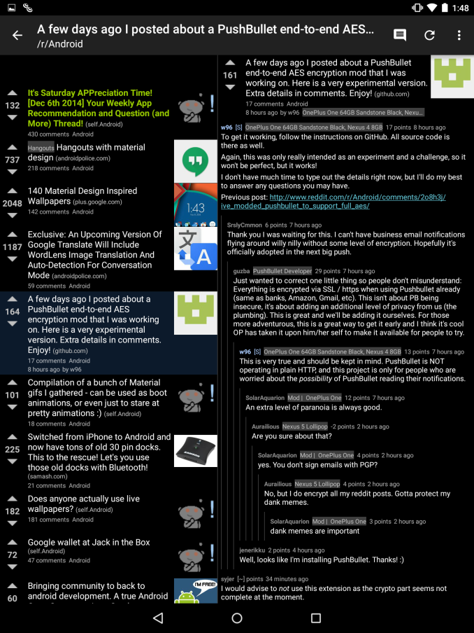
Unfortunately, these seem to be sore points of the Nexus 9 and the broader Android tablet ecosystem. Without question, if we’re talking about tablet applications they definitely do exist for the Nexus 9. The problem is that there is a pervasive lack of applications that are truly designed for a 9 inch, 4:3 aspect ratio display. Applications like Twitter, Facebook, and other first-party apps are simply blown up versions of the phone application. There is some level of extra content presented, but a lot of applications just don’t scale correctly which wastes a lot of real estate on the display. While we found issue with the Nexus 6’s lack of phablet-specific layouts, this is an even bigger issue on the Nexus 9.
While it’s possible to point fingers at app developers for not supporting Android properly, Google seems to have these problems as well. The settings interface is a single large pane of options, instead of a dual-pane interface that allows for simultaneous navigation of the overall settings and individual settings. The Play Store application is mostly similar in this respect, and the YouTube app is possibly the worst example of these kinds of issues. For example, while there is a tablet-specific video view in landscape, most navigation, search, and video selection is identical to what we see on a smartphone.
Nothing really takes advantage of the screen size other than simply being bigger than before. There aren’t any multi-window modes that exploit the larger screen size, and in general the Nexus 9 doesn’t introduce any new functionality that clearly justifies the need for a bag/backpack to carry it. There are applications that take advantage of the larger display, but these are rare. For the most part though, this is effectively true for most tablets other than the Surface Pro 3 which is effectively in a different category altogether.
On the performance side, the story is better but it isn’t perfect either. Similar to Brandon’s experience with the Nexus 6, I often saw random stutters on animations such as the app drawer or while opening an application. It’s hard to say what the cause is at this point, as the Nexus 6 seems to have similar issues with lag even though the Nexus 5 has none of these issues. One might point to FDE causing worse performance, but even that isn’t quite accurate as a build of Lollipop with FDE disabled didn’t do all that much in the way of solving these problems. Overall though, the experience is somehow less performant than the SHIELD Tablet on Android 5.0, even if these issues mostly present themselves in the form of minor frame drops from time to time. I also noticed that there was a distinct lack of available memory over time, which suggests a memory leak as on reboot launcher redraws effectively disappeared.
While these are significant issues that need to be resolved, the experience isn’t actually as bad as it seems. For what it’s worth, Material Design is a great new design scheme to replace the somewhat dated Holo UI that has been in use since Honeycomb/Android 3.0. While there are issues with the tablet experience, if one is willing to look past these issues they will find that the Nexus 9 is a respectable software experience. There’s also the potential for the Nexus 9 to spur improved tablet experiences, although this would be a slow change that could take years to be meaningful.
Camera
In the case of tablets, cameras have become increasingly important. While it’s still a bit awkware to take photos and video with a tablet, there is still value to having decent cameras on a tablet. For the front-facing camera, it’s pretty clear that there is a lot of value to be had here as the tablet can be a good tool for video conferencing in lieu of a bulky laptop. The rear camera can also have value, but mostly for taking a photo of a whiteboard or simply when opportunity dictates. To fulfill these duties, the Nexus 9 has been outfitted with a rather standard set of cameras. On the rear, we see an 8MP, 1/4 inch format sensor while the front-facing camera has a 1.6MP, 1/5 inch sensor. I’ve included a table of the full camera specs below in the interest of readability.
| Camera Specifications | |||
| Google Nexus 9 | |||
| Front Camera | 1.6MP | ||
| Front Camera - Sensor | OV9760 (1.75µm, 1/5") |
||
| Front Camera - Focal Length | 2.18mm | ||
| Front Camera - Max Aperture | F/2.18 | ||
| Rear Camera - Sensor | IMX219 (1.12 µm, 1/4") |
||
| Rear Camera - Focal Length | 3.097mm (33mm eff) | ||
| Rear Camera - Max Aperture | F/2.4 | ||
This is pretty much par for the course when it comes to tablets. The optics aren’t particularly remarkable in one way or another, as I haven’t noticed any obvious design issues in any of my test photos, and the focal length isn’t excessively long or short. The UI that comes with Google Camera in general is unremarkable as well. This isn’t a slight against it, but the fact that I don’t have anything significant to complain about is a good step forward from the past when the design of the camera UI was a significant friction point in the user experience.
The one issue that I’ve noticed is that the camera’s auto focus and capture speed are significantly worse than what I saw on the iPad Air 2. Unfortunately, it isn’t really possible to have standardized testing here as a tablet can’t be mounted to a tripod for testing. As there isn’t a custom ISP in the Nexus 9, it’s likely that the Tegra ISP isn’t up to scratch here as I noticed that AF speed is similar to what I saw on the SHIELD Tablet despite differing camera modules.
For the most part, there’s not much else to be said about the camera systems on the Nexus 9 as they aren’t quite as heavily focused as one would see in the smartphone space. All that’s left to do is test the cameras themselves.
In this basic test of daytime photo quality, we can see that HTC has done a reasonably good job of processing the image as noise is generally suppressed without an enormous loss of detail. However, there really isn't a lot of detail to speak of in this sensor. There's also a decent amount of dynamic range as there's detail in the shadows but there's no HDR mode to compensate in cases where there is insufficient dynamic range. HTC continues to cap the base ISO to 100, which seems to be a strange move in this situation as the shutter speed is more than high enough to drive the sensor gain even lower.
In this low light scenario, the Nexus 9 effectively falls flat on its face. With an ISO of 3200 and a shutter speed of 1/12s, there's effectively no detail past the first set of steps. Luminance noise is strong and present throughout the image, and color noise also has a tendency to creep in as well. Given the sheer size of the tablet, it's also hard to stably hold the tablet to take a photo despite the relatively fast 1/12s shutter speed. One should really avoid using this to take photos in low light unless there's no other choice.
In video, detail generally tends to be about the same as what one can find in photos, which means that daytime footage should have decent quality but low light rapidly reduces the quality as the sensor gain must increase. In the case of the Nexus 9, we see that video tops out at 1080p30 maximum with no slow motion available, and that the file is in a .3gp format instead of a standard mp4 that most are familiar with. The video itself is encoded with H.264 baseline at 14 Mbps, which is likely to be below the maximum that the encoder can support. There doesn't appear to be any significant level of stabilization in this case, which is a bit disappointing although not entirely surprising. There is also a lot of focus hunting throughout the video, which is quite distracting.
Overall, it seems that the camera on the Nexus 9 is an acceptable one for a tablet, although this would effectively be unacceptable on a high-end smartphone. The camera itself produces decent output in daytime but really suffers in low light due to the small pixel size, relatively narrow aperture, and small sensor. There are also a lot of issues with consistent and reliable auto focus, as it often takes multiple focus runs to get the camera to focus properly on even high contrast objects. Each focus run takes a significant amount of time as well, which hurts the shooting experience when combined with the somewhat long capture latency. I would avoid using this camera unless it is strictly necessary, although it isn't terrible as a camera for cases such as document scanning.
WiFi Performance
On most tablets, WiFi performance is perhaps one of the most crucial parts of the experience as WiFi is often the primary method of connectivity. Without working WiFi, a tablet is basically useless as the only alternative is either cellular (which is quite rare on most tablets) or Ethernet over USB-OTG, which destroys most of the value of a mobile device.
In the case of the Nexus 9, we see that HTC has fitted this device with a BCM4354 WiFi module to enable two spatial stream 802.11ac. Interestingly, there is some evidence to suggest that HTC has also adopted Cypress Semiconductor’s CapSense controller to enable antenna tuning for the WiFi antennas. However, it’s probable that this solution is only for HTC devices without a Qualcomm Gobi modem as we’ve seen the use of the QFE15xx antenna tuner in previous HTC products. In order to test how the Nexus 9’s WiFi solution performs, we turn to iperf on Android to test throughput across the network, and utilize Asus’ RT-AC68U router to ensure that the device under test will be able to reach maximum performance.
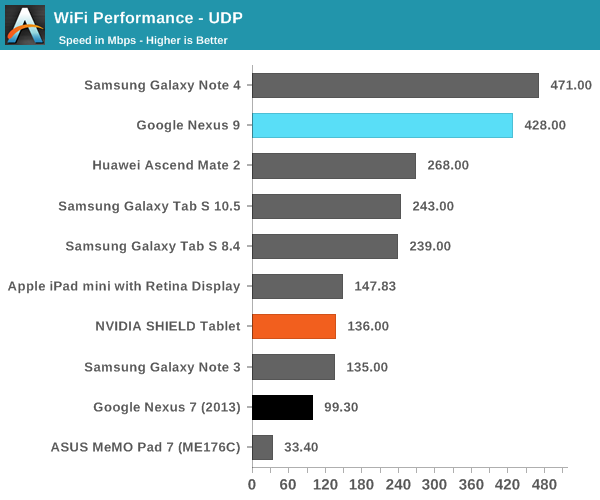
The Nexus 9's WiFi solution performs about as well as one might expect from a BCM4354 solution. For the most part I haven't noticed any reception issues, even when touching/detuning the WiFi antennas.
GNSS
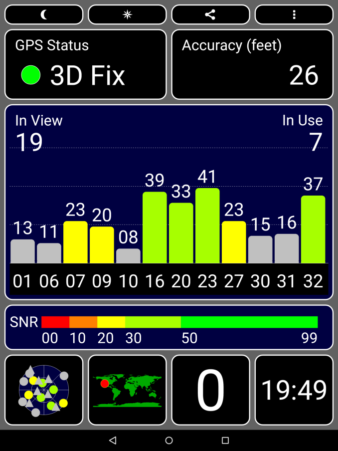
While most of the GNSS solutions that we’ve looked at this year use Qualcomm’s GPSOne/IZat due to the presence of a Qualcomm Gobi Modem, the same isn’t true for the Nexus 9. Instead, Broadcom’s BCM4752 is used here. While this shouldn’t have a massive impact on the speed with which first lock is acquired, in practice Qualcomm’s solution is noticeably faster here as the modem can often provide data to make for a hot fix. At any rate, the Nexus 9 does perform acceptably in this regard. I don’t see any major issues with location performance, although it does seem that the GPS tends to report lower accuracy levels than the Qualcomm solutions that I'm used to. Other than this, the GNSS solution is quite usable.
Misc
While we don't have a proper audio quality test yet, it's clear that the audio codec used is the same Realtek RT5677 codec that we saw in the SHIELD Tablet. Outside of the code, we also see an RT5506 2.55V amp on the 3.5mm jack, along with two NXP TFA9895 amps on the speakers, which are quite good due to their front-facing placement. In practice I don't really see much issue with loudness or quality here, as the speakers can get even louder than the M8 in some situations. We also see a Broadcom BCM2079x NFC chip, which means HCE is fully supported out of the box. Interestingly, the VCM controller is exposed to the OS and is said to be a Texas Instruments DRV201 chip.
Final Words
The Nexus 9 is undoubtedly an aspirational device. For a long time now, Google and the Android tablet market in general have been in a position similar to Amazon’s Fire tablet. This has meant that the margin on the hardware itself has been quite low, and while quality was possible to achieve there were often sacrifices made in order to reach the targeted price point. This was seen in the form of lower CPU and GPU bins in the SoC, lower quality NAND, and generally poorer displays.
The Nexus 7 (2013) did manage to mostly avoid these issues, but Google had set the bar for price and performance to the point where OEMs would have issues with maintaining acceptable profit margins on a device. The Nexus 9 changes this strategy by reaching for a higher price point and attempting to deliver a no-compromise tablet in return. To figure out whether Google has succeeded, it’s worth going over each aspect of the device before coming to any sort of judgment.
The first and quite possibly most important aspect of the Nexus 9 is the SoC. To this end, the Nexus 9 is the very first Android device with AArch64 support enabled in Android. NVIDIA’s Tegra K1 with Denver is effectively the state of the art when it comes to SoCs in the Android OEM space, and no other device has launched with this SoC. While the fact that the SoC is built around the ARMv8 ISA is important, the architecture of the CPU itself is easily one of the most interesting designs we’ve seen in years. Unfortunately, while the design of the CPU is academically interesting it doesn’t seem that this produces real-world benefits. The Nexus 9 has one of the fastest SoCs we’ve seen to date, but this comes at the cost of worse power efficiency than the Cortex A15 version of the Tegra K1.
Another piece of the puzzle is the design, which is one of the key differentiators for a high-end mobile device. While one can debate the merits of various materials, it seems to be clear that an all-metal unibody chassis would’ve greatly improved the design of the Nexus 9 and justified its positioning better. While there is some level of give in the back cover, the buttons are quite thin and hard to find, and there’s a noticeable seam where the back cover and metal frame meet, the design isn’t actually all that bad in practice. Unfortunately, this seems to be a bit of a sore point as well for the Nexus 9 when compared against the iPad lineup.
While the SoC and design are often points of distinction for a premium tablet, the display is critical for any tablet. In this regard, the Nexus 9 does surprisingly well. With a 4:3 aspect ratio, high resolution, and high quality color calibration HTC and Google have outfitted the Nexus 9 with a great display. Unfortunately, there’s a great deal of variability present in these displays that presents itself in the form of backlight bleed along the edges of the display. While my unit only has a slight amount of bleed along the top edge of the device, other units can have more or less backlight bleed depending upon variance in production.
The one aspect that seems to be the product of a poor design choice is the high reflectivity of the display. Although I’m reasonably sure that the display is laminated due to the lack of an obvious gap between the display and glass, it seems that the optical material between the display and glass is poorly designed as I can see a distracting double reflection in the display. The Nexus 9 also compares unfavorably to the iPad Air 2 in this case as the anti-reflective coating on the iPad Air 2 is far superior to just about anything I’ve seen on the market.
Although I previously noted that the power efficiency of the SoC isn’t up to scratch, overall battery life is quite good on the Nexus 9. With a combination of a large battery and efficient display, Google and HTC have managed to compensate for the power consumption issues that come with Denver’s performance. Unfortunately, it seems that Kepler’s desktop-first design results in worse power efficiency than what we see on competing solutions such as the “GXA6850” found in competing SoCs. Even if this is compensated for by the ability to enable desktop-class gaming, the Nexus 9 doesn’t appear to support full OpenGL to begin with, unlike the SHIELD Tablet. This means that the extra capabilities enabled by the GPU are effectively wasted, which hurts the value proposition for the device overall. In light of the launch of the Tegra X1, I can't help but wonder how different the experience of the Nexus 9 would be with NVIDIA's latest SoC.
Outside of these primary elements of the tablet, there seems to be a reasonable level of attention to detail. The camera is acceptable, even if the focus and capture latency aren’t the greatest. The audio quality from the speakers is also quite good, and really helps to enable a great experience when watching any kind of video or listening to music without earbuds/headphones. The software experience is acceptable, although Google continues to fight issues with ecosystem support for tablets.
With all of this in mind, it’s hard to give a resounding recommendation of the Nexus 9. The Nexus 9 is a step towards a high-end Android tablet, but not the leap that Google was hoping for. If you want an Android tablet near the size of the Nexus 9, I can’t really recommend anything else. The Galaxy Tab S falls short on account of performance and battery life, and despite the somewhat unremarkable design of the Nexus 9 I believe that it is nicer than the Galaxy Tab S. However, if one were to assume that OEMs are currently readying devices to truly carry the torch of the high-end tablet, the Nexus 9 is a hard sell. I suspect that this wouldn’t be nearly as difficult if the Nexus 9 had a lower price point of $300 and $350 USD for the 16GB and 32 GB WiFi variants, and $450-$500 for the 32GB LTE variant. Google has managed to get close to the mark with the Nexus 9, but like the Nexus 6 it seems that it’s up to the OEMs to cover the remaining distance.

