Testing Samsung 850 Pro Endurance & Measuring V-NAND Die Size
by Kristian Vättö on July 7, 2014 1:20 PM ESTV-NAND Die Size: Bigger Than What We Initially Thought
In our 850 Pro review, I did some calculations to estimate the die size of the second generation V-NAND based on the first generation V-NAND. As some of our clever readers pointed out, the die size does not scale perfectly with the die capacity because the peripheral circuitry cannot be scaled as aggressively as the capacity can be. As a result, my initial estimation ended up being way too small because I did not take the scaling of the peripheral circuitry into account.
Unfortunately, Samsung would not disclose the die size during the Q&A at the SSD Global Summit so I had to seek for an alternative way to figure out the correct die size. In the showroom, Samsung had the second generation 32-layer V-NAND wafer, which actually gives us everything we need to calculate a fairly accurate estimation of the die size.
The picture on top shows what the wafer looks like. It does not look any different from the typical 2D NAND wafer, which should not be a surprise given that the change happened deep inside. And no, the V-NAND wafer is not thicker than any normal wafer (at least not by eye) because the V-NAND stack is still in the order of microns.
As for the die size, I calculated 44 dies in the vertical direction, which means that with a 300mm wafer the depth of a single die is approximately 6.8mm.
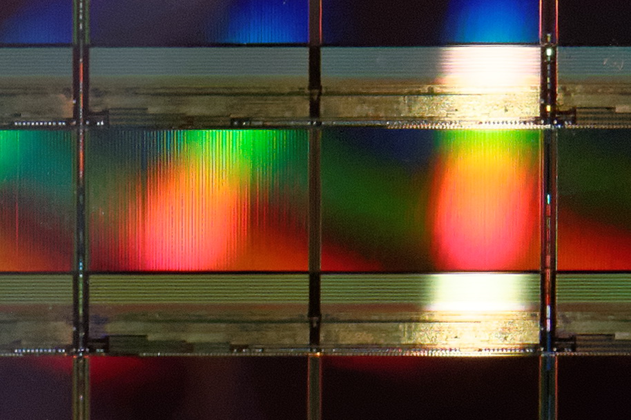
Courtesy of PC Perspective
To figure out the width of the die, you can either count the dies in the horizontal direction or go with the lazy route and just calculate the proportion of the depth and width. Allyn Malventano from PC Perspective was able to grab this awesome photo of the die itself, so I used the ruler tool in Photoshop to measure the size of the die along both X and Y axes and it appears that the width of the die is about 2.05 times its depth (note that it is a two-plane design). In other words, the die size is around 6.8mm x 14.0mm, which works out to be 95.4mm2.
| NAND Die Comparison | ||||
| Samsung 1st Gen V-NAND | Samsung 2nd Gen V-NAND | Micron 16nm NAND | Toshiba A19nm NAND | |
| Die Capacity | 128Gbit | 86Gbit | 128Gbit | 64Gbit |
| Die Size | 133mm2 | ~95.4mm2 | 173mm2 | 94mm2 |
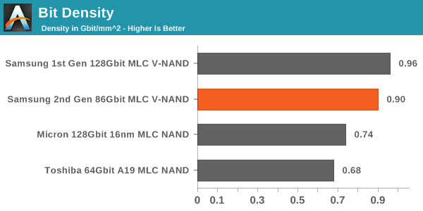
Here is an updated bit density graph. Even with the updated, larger die size, V-NAND is noticeably denser than 2D NAND, although the first generation appears to be more dense. I am guessing the smaller die size is better for yields (larger chips have higher probability of manufacturing errors), which makes the second generation more cost efficient despite the slightly lower density.


39 Comments
View All Comments
jjj - Monday, July 7, 2014 - link
You shouldn't assume that it makes sense from a cost perspective. Samsung is huge and sometimes it might focus less on cost ,maybe it's a commercial beta for now and they are not quite where they need to be.As for per layer you have 128Gb in 24 layers and 86Gb in 32 layers so a layer is 5.3333 Gb and 2.6875Gb and if you factor in die size the difference seems strangely high.
jjj - Monday, July 7, 2014 - link
Double posting here but just remembered,that i always wondered about temps for 3D NAND so , have you looked at heat and how it compares with 2D?Kristian Vättö - Monday, July 7, 2014 - link
Sure it's possible that Samsung is just "playing around with 32-layer design" but after all Samsung is a company with a target to generate profit for the shareholders. There must be a reason why Samsung didn't just add eight layers to the first Gen design and make it a ~170Gbit chip with about the same die size.Here are some numbers I crushed:
Die Size: 133mm^2 (1st gen) - 95.4mm^2 (2nd gen)
Observed Array Efficiency: 85% - 64%
Die Area Dedicated to Arrays: 113.1mm^2 - 61.1mm^2
Array Density: 1.13Gbit/mm^2 - 1.41Gbit/mm^2
Array Density per Layer: 0.047Gbit/mm^2 - 0.044Gbit/mm^2
In other words, when you take all the factors into account, it all adds up. Sure there is still a ~10% difference but nearly everything we have is estimations, so a 10% error sounds fair.
jjj - Monday, July 7, 2014 - link
Obviously smaller is most likely for yields reasons but it's not enough to draw the conclusion that cost per bit got better. I'm also not very sure how perf and power and heat changed from first gen to second, that's also a factor to consider when deciding to go this way.It is very likely that the first gen wasn't cost effective compared to 2D and all the other 3 big players are not jumping in just yet because of cost and that would suggest that for Samsung cost wasn't the main factor when they decided to launch 3D. As far as we can tell 3D is pretty low volume for now so the cost might matter very little for someone like Samsung. An objective could be to advance the technology while gaining share in enterprise SSD and enhancing the brand's image.
Second gen cost per bit could be better already or they could hope to get there soon but we just don't have the data to draw any conclusion.
jjj - Monday, July 7, 2014 - link
Looked at the numbers, i guess by looking at the area dedicated to the arrays there is only a small enough difference.Would be really nice to have some yield and cost projections based on die size, layers and process to try to figure out what the next steps will be.Second gen seems rather small given the array efficiency so maybe they'll aim for something bigger in gen 3. I am already dreaming of 140mm2 48 layer on 28nm at 512Gb at some point soon(ish).
repoman27 - Monday, July 7, 2014 - link
Some back of the envelope calculations show that the 2nd gen V-NAND would provide 6% fewer total bits per wafer, echoing your bit density calculations, but would come in the form of 40% more dies. If you expect even moderate issues with defects, that could make the 2nd gen much more profitable to produce, or simply a hedge as they ramp the number of layers with a relatively novel process.Samsung is pretty good at die stacking, but the other aspect may have to do with the smaller dies being much easier to stack in a standard 12 or 14 x 18mm package.
Per Hansson - Monday, July 7, 2014 - link
I'm having a hard time understanding the correlation of these numbers.A friend has a Intel X25-M G2 80GB drive that according to the SMART data has logged 73TB host writes.
That SSD has become slow, when testing using AS SSD it logs 1000ms on read access time for example.
Yet still the "media wearout indicator" is only at 97, implying the SSD has only used up 3% of it's life.
However the drive is warranted by Intel at a maximum of 7.5TB, so how do these numbers relate?
extide - Tuesday, July 8, 2014 - link
Speed and age have nothing to do with each otherextide - Tuesday, July 8, 2014 - link
Well, not nothing, but little enough that it is essentially nothing. The speed difference you are seeing are due to fragmentation at various levels. A secure erase would restore the drive to like-new speed.Per Hansson - Tuesday, July 8, 2014 - link
Thank you so much extide for your insight!I created a Ghost backup of the drive and did a secure erase (took a while to find a computer where hdderase.exe would work, and which would release the security frozen lock)
But once I did and restored the Ghost the drive is almost like new, write performance more than doubled and read access time went from ~1000ms to ~180ms
I also found another interesting thing out and that was by upgrading Intel SSD Toolbox from v3.1.6 to v3.2.1 the value "E1 Host Writes" went from 73TB down to 7.57TB (None of the other SMART values changed)
The Windows Experience Index score also went from 5.9 > 7.7
So far this SSD has 4.5 years of power on hours logged, so it's quite well used, only 96 power cycles, would be allot more without the UPS :)