Intel Unveils Meteor Lake Architecture: Intel 4 Heralds the Disaggregated Future of Mobile CPUs
by Gavin Bonshor on September 19, 2023 11:35 AM EST
During the opening keynote at Intel's Innovation event in San Jose, Chief Executive Officer Pat Gelsinger unveiled a score of details about the upcoming Meteor Lake client platform. Intel's Meteor Lake marks the beginning of a new era for the chipmaker, as they move away from the chaotic Intel 7 node and go into a rollout of their Foveros 3D packaging with EUV lithography for their upcoming client mobile platform. Meteor Lake uses a tiled, disaggregated chiplet architecture for its client-centric processors for the first time, changing the very nature of Intel's consumer chips going forward. And, according to Intel, all of these changes have allowed them to bring some significant advancements to the mobile market.
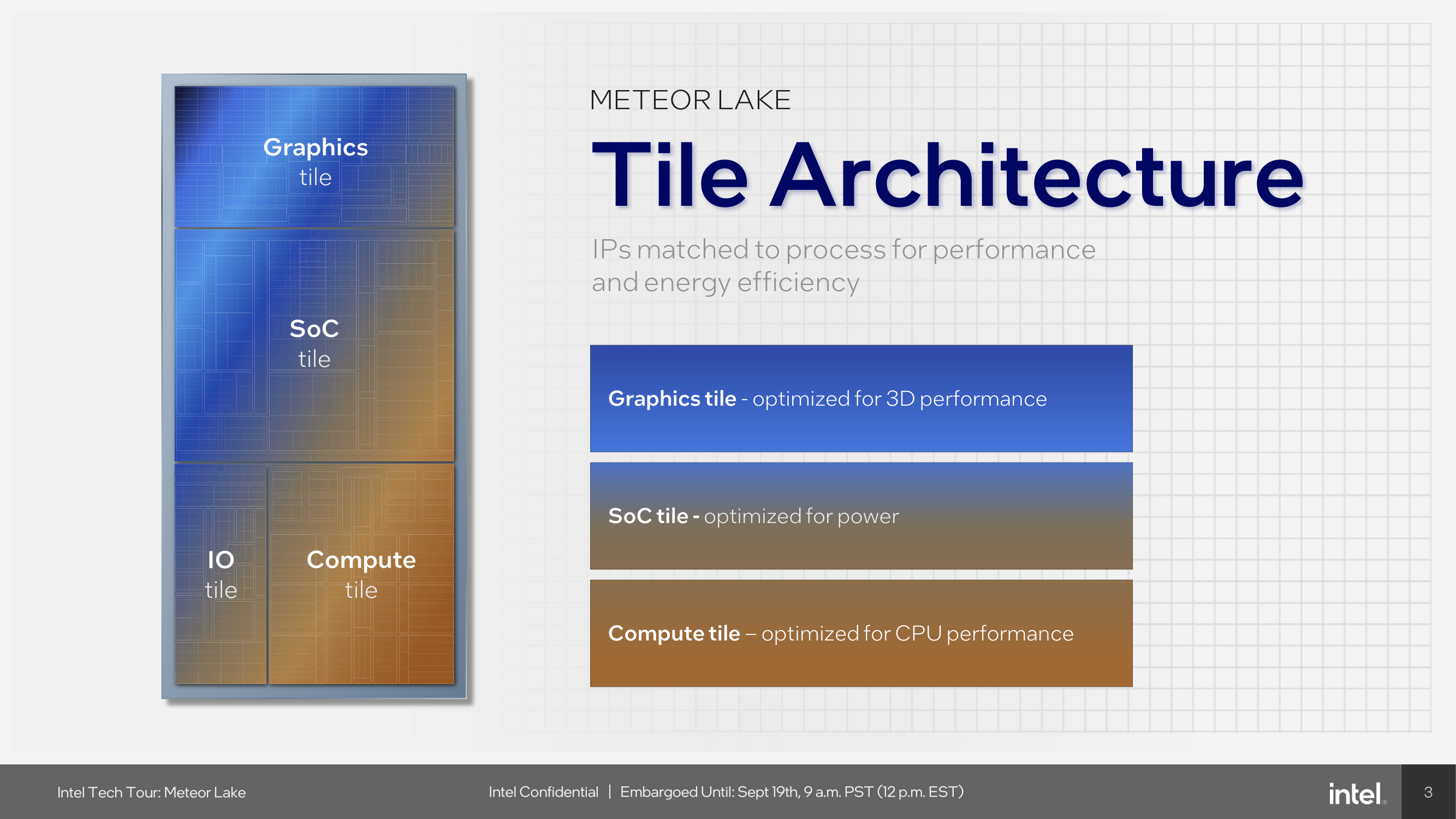
Intel's first chiplet-based consumer CPU breaks up the common functions of a modern CPU into four individual tiles: compute, graphics, SoC, and an I/O tile. Within the makeup of the compute tile is a new pair of cores, a P-core named Redwood Cove and a new E-core called Crestmont. Both these cores promise IPC gains over their previous counterparts, but perhaps the most interesting inclusion is a new type of E-core embedded directly into the SoC tile, which Intel calls 'Low Power Island.' These new LP E-cores are designed with the idea that light workloads and processes can be taken off the more power-hungry compute tile and offloaded onto a more efficient and lower-powered tile altogether. Other major additions include a first-for-Intel Neural Processing Unit (NPU), which sits within the SoC tile and is designed to bring on-chip AI capabilities for workloads and inferencing, paving the way for the future.
With Meteor Lake, Intel is aiming to put themselves in a more competitive position within the mobile market, with notable improvements to compute core hierarchy, Intel's Xe-LPG Arc-based graphics tile looking to bolster integrated graphics capabilities, and an NPU that adds various AI advantages. Meteor Lake also sets the scene for Intel and modular disaggregation, with Foveros 3D packaging set to become a mainstay of Intel's processor roadmap for the future, with the Intel 4 process making its debut and acting as a stepping stone to what will become Intel's next mainstay node throughout its fabs, Intel 3.
Intel Meteor Lake: Intel 4 Using Foveros 3D Packaging
Intel's Meteor Lake architecture is not just another iteration in the long line of processor advancements; according to the company it's a revolutionary leap forward. Eloquently put by the executive VP and GM of Intel's Client Computing Group (CCG), Michelle Johnston Holhaus, at Intel's Tech Tour 2023 in Penang, Malaysia, she remarked that Intel had reached an inflection point in their client roadmap. Unveiling more details about Meteor Lake at the Intel Technology Tour in Malaysia, the architecture is an advancement from its current client processors regarding performance as we advance through Intel's '5 nodes in 4 years' roadmap.

Meteor Lake is built upon Intel's disaggregated architecture pushed through by Foveros packaging. This is designed to optimize both performance and energy efficiency. The architecture itself consists of four unique and distinct tiles connected via Intel's Foveros 3D packaging technology. This includes the compute tile, which is built on Intel 4, while the graphics tile is built on TSMC's N5 node. The other two tiles Intel implements within Meteor Lake are the SoC tile which acts as the central hub through the embedded NOC. This is the first time Intel has used a Network-on-Chip (NOC) on their client processors, which is a simplified approach to the NOC on their existing Agilex FPGAs. While on Agilex, the NOC is individualized into different NoC targets and switches within the substructure of the NoC, on Meteor Lake, it directly connects to the I/O fabric through the IoC, which then goes into the I/O fabric. The NOC itself is directly connected to the graphics tile, compute tile, and other components within the SoC.
This modular approach allows for a ground-up and scalable power management architecture that supports disaggregation, enabling each tile to function independently. This disaggregated design prioritizes performance by negating bandwidth bottlenecking through things like the I/O on a monolithic design and targets enhanced power efficiency. Perhaps the most notable element of disaggregation is that Intel can select specific silicon processes for each tile and isn't limited to one process node. On top of the power efficiency and package area benefits of a tiled architecture, it is cheaper for Intel to manufacture CPUs with fewer masks through EUV, but it allows Intel to scale out new IP into future products while keeping the same base, which is another cost-saving factor (for Intel).
Compared to mobile Raptor Lake, which was done using Multi-Chip Packaging (MCP), Meteor Lake uses Foveros BGA packaging and offers low-power die-to-die interconnects, which Intel confirmed has a small power penalty of between 0.15 and 0.3 picojoules (pJ) communicating from tile to tile. Some of the advantages of Foveros include better customizability through tiling, which allows Intel to manufacture chips and implement specific tiles and IP depending on the grade of the chip, etc., low power with more I/O, or high-end tiles with all the latest gadgets and gizmos. With the Intel 7 node not being as viable as they would have hoped, Intel promises higher wafer yield on Intel 4, which uses less wafer space for logic-based silicon.
Power management is done using a scalable power management system that supports the independent functioning of each tile. Coordination between multiple power management controllers (PMC) and system software is designed to be optimized for various workloads. Intel's Meteor Lake architecture also introduces a new scalable fabric to improve energy efficiency and extend bandwidth in areas that have been previously bottlenecked, such as I/O.
Touching more on the power controllers within the Meteor Lake architecture, Intel has integrated independent Power Management Controllers within each of the tiles. As part of the disaggregation of using Foveros, each tile needs to be independently power managed, and using PMCs on the NOC, the I/O fabric, as well as each tile allows power management to be agnostic depending on the number of the cores on each package.
Meteor Lake itself represents a monumental architectural shift, not just a mere incremental update, as it represents the most significant architectural transformation in client processors in four decades. This is because it's the first client processor to be made using chiplets instead of a monolithic design. The architecture is designed to be the cornerstone of Intel's strategy to push PC innovation for the next decade. Looking at some of the finer details of Intel's Meteor Lake architecture, it uses Intel's Foveros packaging technology, which uses 3D chip stacking to tackle the pitfalls of traditional 2D chip layouts.
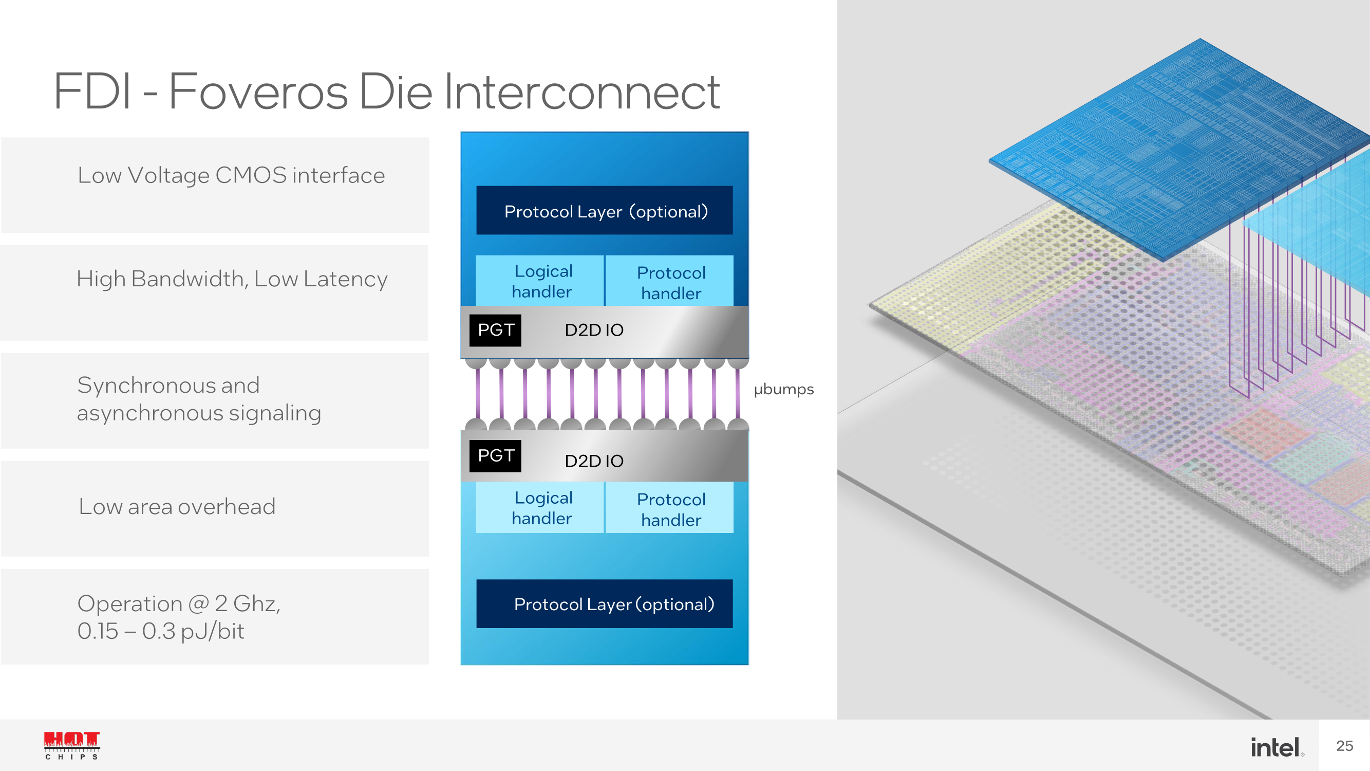
As we can see from the above disclosure from Intel at Hot Chips 2023, the top and bottom layers have bumps for interconnecting each die together. Using the Foveros FDI packaging offers a low-voltage complementary metal oxide semiconductor (CMOS) interface, which means the power circuitry can be run with lower voltages and, thus, with a lower power envelope. Another benefit of FDI is both synchronous and asynchronous signaling, which means signal transmission can handle fully duplexed data blocks.
Constructing a Meteor Lake SoC includes a package substrate, which is the foundation for the base tile to sit onto, which uses the Foveros Die Interconnect (FDI). The base tile has a 36µm die to die pitch with metal layering and a 0.15 to 0.3 pJ operating power at 2 GHz; this may fluctuate or vary depending on voltages, amps, and frequency. As it's a base tile that isn't an active chiplet itself, its only function is to serve as a base for all of the various logic, and metal layers for the chiplets to be placed upon.
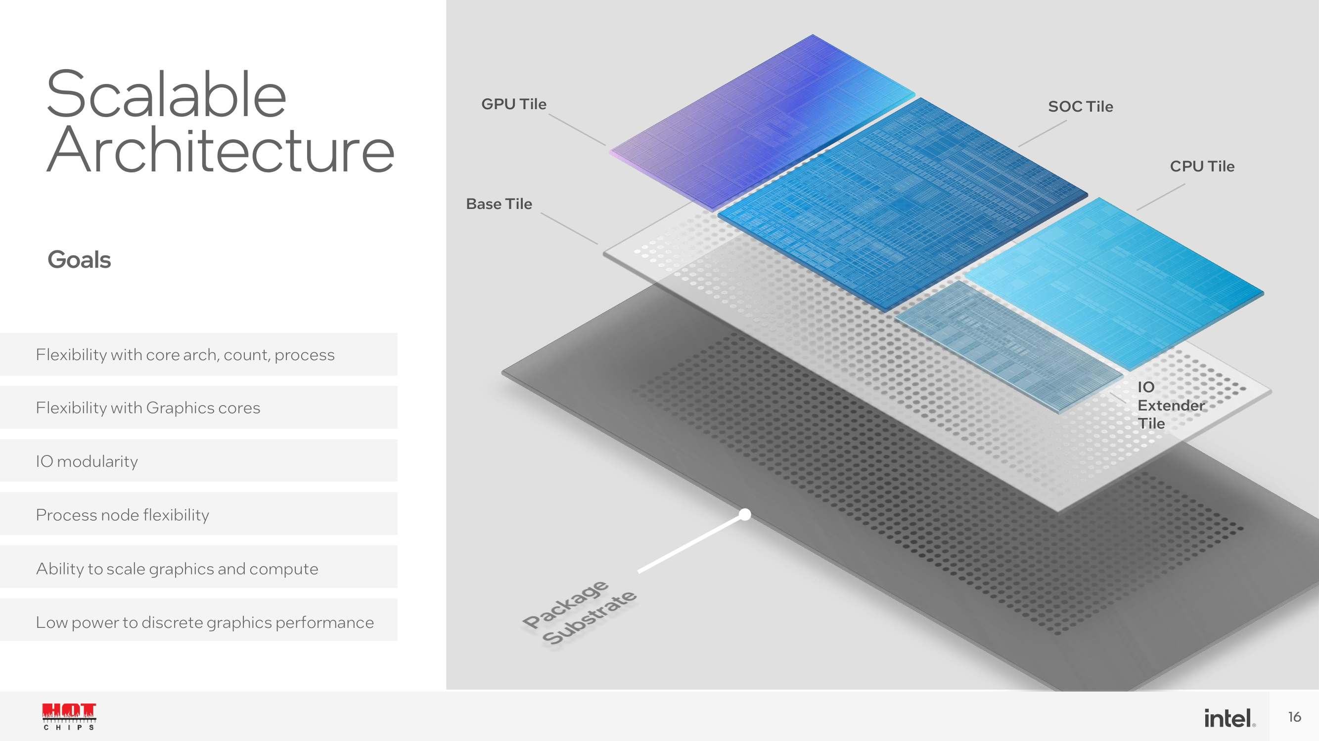
The makeup of Intel's Meteor Lake architecture uses four distinct tiles to create a Meteor Lake CPU. This includes a Compute, SoC, GPU, and an I/O tile, all with distinct uses, capabilities, and flexibility in regard to IP. Power management also gets a revamp. With disaggregation through Intel's Foveros packaging technology, each tile in Meteor Lake requires its own power management. Intel's solution is a hierarchical power management system that uses Power Management Controllers on the NoC, IO fabric, and each individual tile.
Over the next few pages, we'll give an insight into each of the four tiles, what each tile brings to the table, and more about the various technologies driving innovation through Meteor Lake.


107 Comments
View All Comments
Composite - Thursday, September 28, 2023 - link
totally agree. At the same time, instead of doing a full Intel 4 Meteor lake chip, shrink it down to compute tile only also reduces the size of the silicon and improves yield. Later next year, Intel will also need EUV capacity for Sierra Forest and Granite Rapids. These chips will be much larger than mobile compute tile and considerably lower yield.... Intel will need every ounce of EUV capacity they have.tipoo - Tuesday, September 19, 2023 - link
Probably to have as much compute on the N4 capacity that they have, their substrate also takes much less power connecting them than current AMD and it allows for the best node for each part being used i.e if Intel's wasn't ideal for the GPU tile as the CPU tile etcComposite - Thursday, September 28, 2023 - link
I have the same question. At the same time, I was curious about Intel's EUV capacity. Since Intel is the late comer to EUV and over 50% of EUV machines are at TSMC, does Intel really have the capacity to manufacture full chip Intel 4 Meteor Lake? Not to mention up coming Sierra Forest and later on Granite Rapids will all use EUV capacity. I think the reasonable way is indeed only use EUV at the most critical part of Meteor Lake ---> Compute tile, and out source the rest.eSyr - Tuesday, September 19, 2023 - link
To avoid the issues they have with rollout 14 nm (BDW) and then 10 nm (CNL), I guess, when they held back by yield with respect to particular parts of the chip, specifically, GPU.lemurbutton - Tuesday, September 19, 2023 - link
A17 Pro just beat all Intel CPUs except the 13900KS in ST Geekbench6. A17 Pro uses less than 3w to achieve this - with typical load significantly below 3w. Meanwhile, 13900KS uses as much as 250w or more.Intel's Meteor Lake needs to improve by 10x over Raptor Lake just to match what M3 will be able to do.
Irish_adam - Tuesday, September 19, 2023 - link
The 13900ks uses 250 watts on a single core? Got a link for that?I'll think you find that single core workloads use far, far less. Also remember that benchmarks across ISA's are sketch at best and outright made up at worst. I mean just look how badly games or software can be when ported from one ISA to another, it all really comes down to how well you've made the software to run on each architecture.
Makaveli - Tuesday, September 19, 2023 - link
He is an apple fanboySource: Trust me bro!
FWhitTrampoline - Tuesday, September 19, 2023 - link
No the A17 Performance core is only clocked at 3.6/3.7GHz compared to the x86 designs that are up to clocked 2Ghz+ higher. So this is not some ESPN like Fanatic statement as since the A14/Firestorm core Apple's instruction decoder width is at least 8 decoders wide and backed up by loads of execution ports. And so Apple's P cores are of a very wide order superscalar design since the A14/Firestorm was released!And the Apple P cores are high IPC at low clocks compared to the x86 designs that have 4/6 instruction decoders so need the higher clocks to make up the IPC deficiency for single thread performance that's calculated as IPC multiplied by average sustained clocks to get that single threaded performance metric.
The lower clocks are where Apple's power savings come from and the longer battery life is obtained. That and the A17 Pro/Earlier A series SOCs have loads of specialized heterogeneous compute for offloading workloads onto instead of using the CPU cores or GPU cores so more power can be saved there for all sorts of specialized workloads. The x86 processors/SOCs are just now getting the same sorts of specialized heterogeneous compute IP blocks but that's relatively immature compare to Apple's SOCs and other ARM Based SOC ecosystems that have been using that specialized heterogeneous compute IP for years now.
GeoffreyA - Thursday, September 21, 2023 - link
Well, it would be interesting to see Intel or AMD make a fixed-width ISA design and how that then stacks up against the stuff of Apple. Really, x86 is at a disadvantage because of the variable-width instructions but still has done a fantastic job. Or, I'd like to see Apple design an x86 CPU and see how that holds up against Zen and the rest.FWhitTrampoline - Thursday, September 21, 2023 - link
No logical reason for Apple to go CISC as the x86 Instruction Decoder requires many times the transistors to implement than the transistors required to implement a RISC ISA Instruction Decoder! So it was easy to get 8 Instruction Decoders to fit on the front of the A14/Firestorm processor core(RISC ISA Based). It's easier to go wider if one has a relatively fewer Instructions of a fixed length to implement in a Instruction Decoder design. So that makes it easy to produce a custom very wide order superscalar processor core design that targets high IPC at a lower clock rate and the SOC's CPU cores clocked well inside their Performance/Watt sweet spot. And to still have that A14 match/get close to the x86 cores in single threaded performance and against x86 core designs that are clocked 2GHz+ higher.The x86 ISA is too Legacy Instructions bloated and it's not going to be easy to refactor that and not require years in the process to do that. The ARM ISA ecosystem is from the ground up RISC there and even though the x86 designers have a RISC like back end to break those CISC down into more RISC like instructions, that hardware engine take more transistors to implement and thus will use more power resources getting that done. The vast majority of ARM ISA instructions translate 1 to 1 into single and some a few Micro-OPs so how hard is that to decode compared to x86 ISA instruction that mostly have multiple micro-ops generated to get all that complex work done. And there's a valid power usage reason that x86 never made any inroads into the wider tablet/smartphone market.
The thing about the ARM/RISC core designs is that they can scale from phones to server/HPC whereas the CISC designs can not scale down as low power as RISC designs! but Intel has done a good job at getting close there but a little too late to matter to the OEMs that really did not want to remain beholden to Intel and x86. And the same can be said now for RISC-V compared to an ARM Holdings that's maybe leaning more towards an x86 like business model where RISC-V represents total end user ISA freedom there, within reason, as the RISC-V ISA is totally open not royalist/encumberments required/enforced.