Intel Unveils Meteor Lake Architecture: Intel 4 Heralds the Disaggregated Future of Mobile CPUs
by Gavin Bonshor on September 19, 2023 11:35 AM EST
During the opening keynote at Intel's Innovation event in San Jose, Chief Executive Officer Pat Gelsinger unveiled a score of details about the upcoming Meteor Lake client platform. Intel's Meteor Lake marks the beginning of a new era for the chipmaker, as they move away from the chaotic Intel 7 node and go into a rollout of their Foveros 3D packaging with EUV lithography for their upcoming client mobile platform. Meteor Lake uses a tiled, disaggregated chiplet architecture for its client-centric processors for the first time, changing the very nature of Intel's consumer chips going forward. And, according to Intel, all of these changes have allowed them to bring some significant advancements to the mobile market.
Intel's first chiplet-based consumer CPU breaks up the common functions of a modern CPU into four individual tiles: compute, graphics, SoC, and an I/O tile. Within the makeup of the compute tile is a new pair of cores, a P-core named Redwood Cove and a new E-core called Crestmont. Both these cores promise IPC gains over their previous counterparts, but perhaps the most interesting inclusion is a new type of E-core embedded directly into the SoC tile, which Intel calls 'Low Power Island.' These new LP E-cores are designed with the idea that light workloads and processes can be taken off the more power-hungry compute tile and offloaded onto a more efficient and lower-powered tile altogether. Other major additions include a first-for-Intel Neural Processing Unit (NPU), which sits within the SoC tile and is designed to bring on-chip AI capabilities for workloads and inferencing, paving the way for the future.
With Meteor Lake, Intel is aiming to put themselves in a more competitive position within the mobile market, with notable improvements to compute core hierarchy, Intel's Xe-LPG Arc-based graphics tile looking to bolster integrated graphics capabilities, and an NPU that adds various AI advantages. Meteor Lake also sets the scene for Intel and modular disaggregation, with Foveros 3D packaging set to become a mainstay of Intel's processor roadmap for the future, with the Intel 4 process making its debut and acting as a stepping stone to what will become Intel's next mainstay node throughout its fabs, Intel 3.
Intel Meteor Lake: Intel 4 Using Foveros 3D Packaging
Intel's Meteor Lake architecture is not just another iteration in the long line of processor advancements; according to the company it's a revolutionary leap forward. Eloquently put by the executive VP and GM of Intel's Client Computing Group (CCG), Michelle Johnston Holhaus, at Intel's Tech Tour 2023 in Penang, Malaysia, she remarked that Intel had reached an inflection point in their client roadmap. Unveiling more details about Meteor Lake at the Intel Technology Tour in Malaysia, the architecture is an advancement from its current client processors regarding performance as we advance through Intel's '5 nodes in 4 years' roadmap.

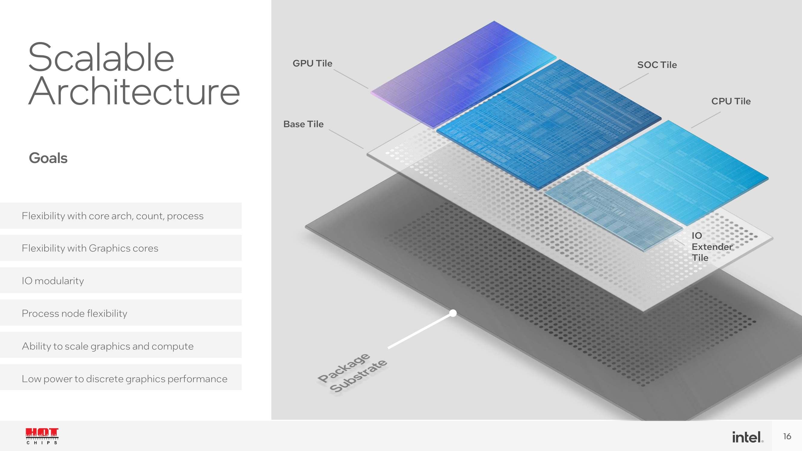
Meteor Lake is built upon Intel's disaggregated architecture pushed through by Foveros packaging. This is designed to optimize both performance and energy efficiency. The architecture itself consists of four unique and distinct tiles connected via Intel's Foveros 3D packaging technology. This includes the compute tile, which is built on Intel 4, while the graphics tile is built on TSMC's N5 node. The other two tiles Intel implements within Meteor Lake are the SoC tile which acts as the central hub through the embedded NOC. This is the first time Intel has used a Network-on-Chip (NOC) on their client processors, which is a simplified approach to the NOC on their existing Agilex FPGAs. While on Agilex, the NOC is individualized into different NoC targets and switches within the substructure of the NoC, on Meteor Lake, it directly connects to the I/O fabric through the IoC, which then goes into the I/O fabric. The NOC itself is directly connected to the graphics tile, compute tile, and other components within the SoC.
This modular approach allows for a ground-up and scalable power management architecture that supports disaggregation, enabling each tile to function independently. This disaggregated design prioritizes performance by negating bandwidth bottlenecking through things like the I/O on a monolithic design and targets enhanced power efficiency. Perhaps the most notable element of disaggregation is that Intel can select specific silicon processes for each tile and isn't limited to one process node. On top of the power efficiency and package area benefits of a tiled architecture, it is cheaper for Intel to manufacture CPUs with fewer masks through EUV, but it allows Intel to scale out new IP into future products while keeping the same base, which is another cost-saving factor (for Intel).
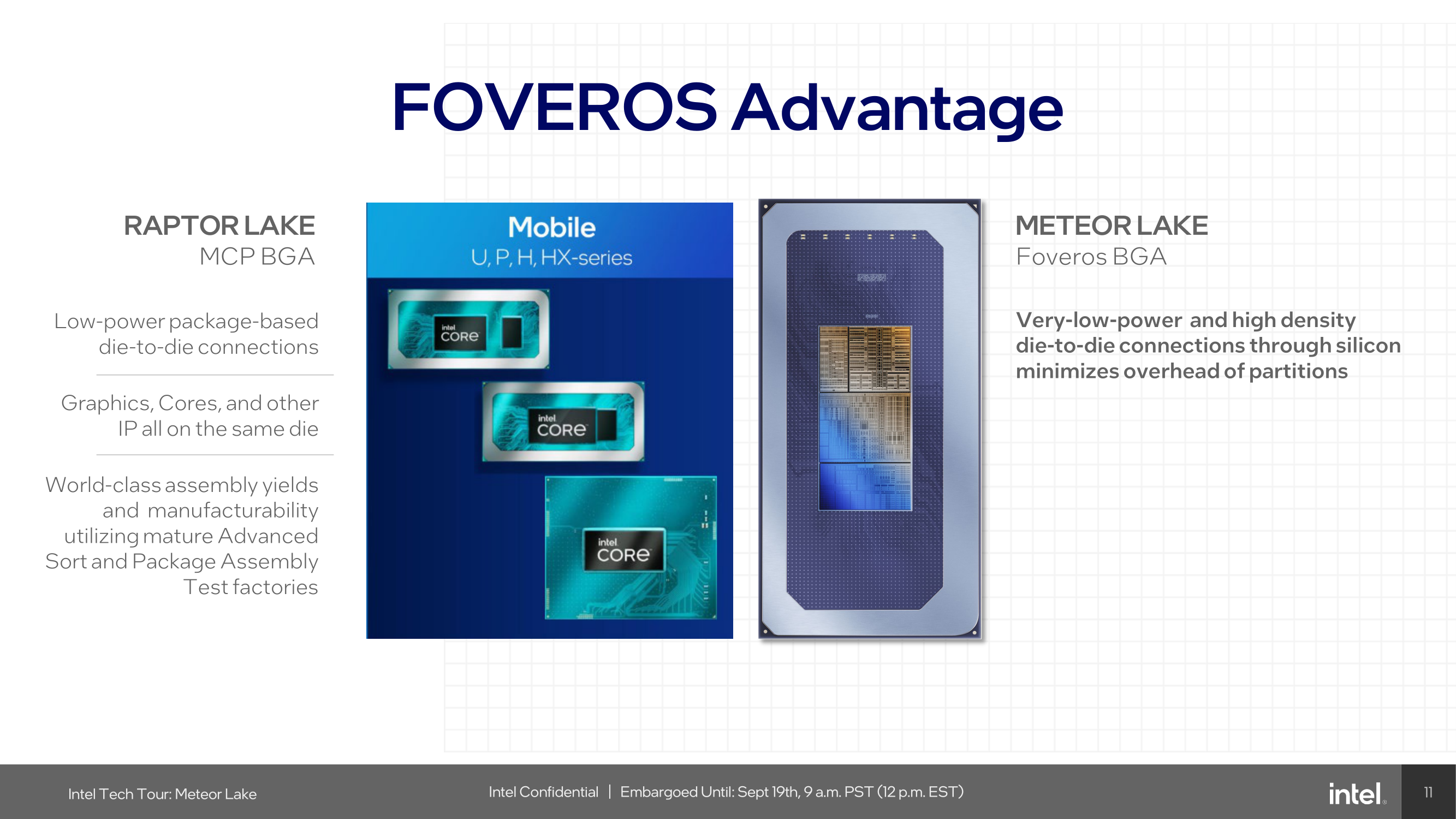
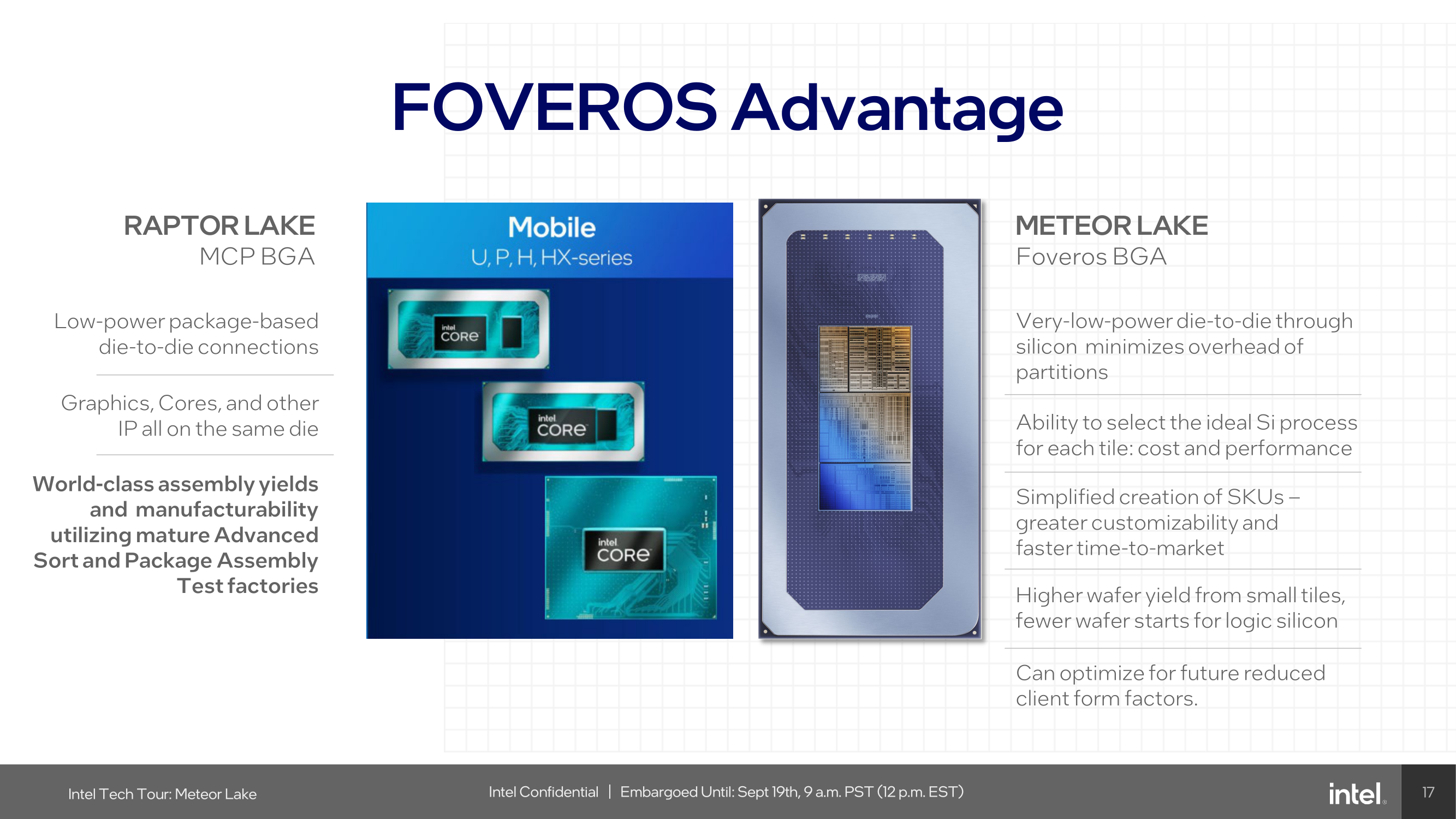
Compared to mobile Raptor Lake, which was done using Multi-Chip Packaging (MCP), Meteor Lake uses Foveros BGA packaging and offers low-power die-to-die interconnects, which Intel confirmed has a small power penalty of between 0.15 and 0.3 picojoules (pJ) communicating from tile to tile. Some of the advantages of Foveros include better customizability through tiling, which allows Intel to manufacture chips and implement specific tiles and IP depending on the grade of the chip, etc., low power with more I/O, or high-end tiles with all the latest gadgets and gizmos. With the Intel 7 node not being as viable as they would have hoped, Intel promises higher wafer yield on Intel 4, which uses less wafer space for logic-based silicon.
Power management is done using a scalable power management system that supports the independent functioning of each tile. Coordination between multiple power management controllers (PMC) and system software is designed to be optimized for various workloads. Intel's Meteor Lake architecture also introduces a new scalable fabric to improve energy efficiency and extend bandwidth in areas that have been previously bottlenecked, such as I/O.
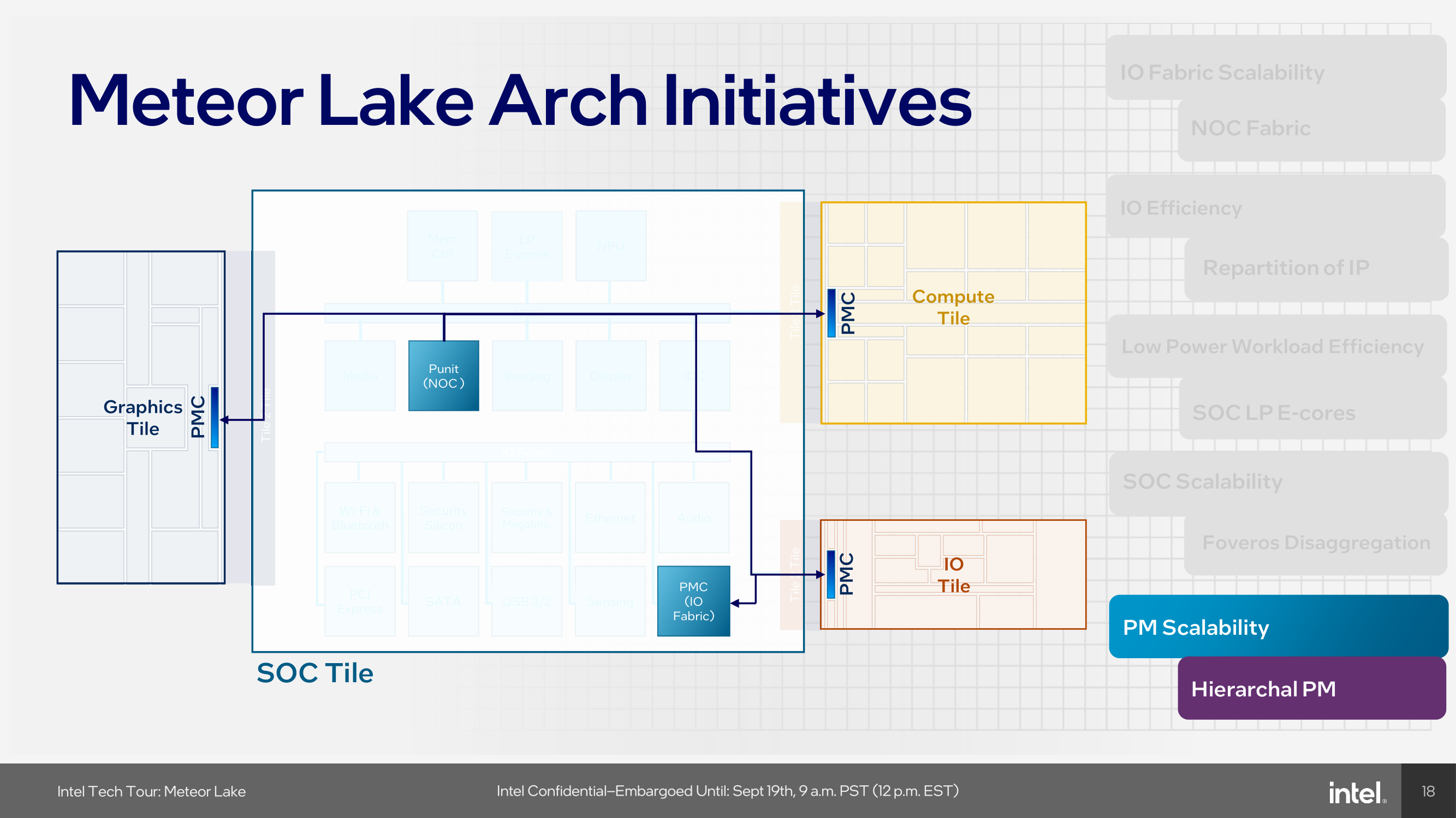
Touching more on the power controllers within the Meteor Lake architecture, Intel has integrated independent Power Management Controllers within each of the tiles. As part of the disaggregation of using Foveros, each tile needs to be independently power managed, and using PMCs on the NOC, the I/O fabric, as well as each tile allows power management to be agnostic depending on the number of the cores on each package.
Meteor Lake itself represents a monumental architectural shift, not just a mere incremental update, as it represents the most significant architectural transformation in client processors in four decades. This is because it's the first client processor to be made using chiplets instead of a monolithic design. The architecture is designed to be the cornerstone of Intel's strategy to push PC innovation for the next decade. Looking at some of the finer details of Intel's Meteor Lake architecture, it uses Intel's Foveros packaging technology, which uses 3D chip stacking to tackle the pitfalls of traditional 2D chip layouts.
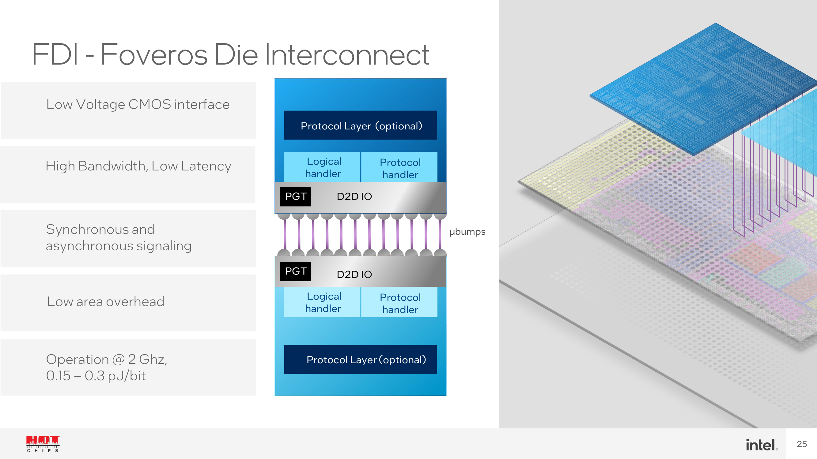
As we can see from the above disclosure from Intel at Hot Chips 2023, the top and bottom layers have bumps for interconnecting each die together. Using the Foveros FDI packaging offers a low-voltage complementary metal oxide semiconductor (CMOS) interface, which means the power circuitry can be run with lower voltages and, thus, with a lower power envelope. Another benefit of FDI is both synchronous and asynchronous signaling, which means signal transmission can handle fully duplexed data blocks.
Constructing a Meteor Lake SoC includes a package substrate, which is the foundation for the base tile to sit onto, which uses the Foveros Die Interconnect (FDI). The base tile has a 36µm die to die pitch with metal layering and a 0.15 to 0.3 pJ operating power at 2 GHz; this may fluctuate or vary depending on voltages, amps, and frequency. As it's a base tile that isn't an active chiplet itself, its only function is to serve as a base for all of the various logic, and metal layers for the chiplets to be placed upon.
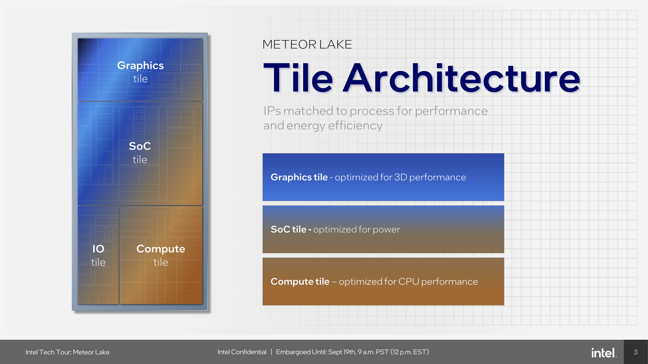
The makeup of Intel's Meteor Lake architecture uses four distinct tiles to create a Meteor Lake CPU. This includes a Compute, SoC, GPU, and an I/O tile, all with distinct uses, capabilities, and flexibility in regard to IP. Power management also gets a revamp. With disaggregation through Intel's Foveros packaging technology, each tile in Meteor Lake requires its own power management. Intel's solution is a hierarchical power management system that uses Power Management Controllers on the NoC, IO fabric, and each individual tile.
Over the next few pages, we'll give an insight into each of the four tiles, what each tile brings to the table, and more about the various technologies driving innovation through Meteor Lake.


107 Comments
View All Comments
FWhitTrampoline - Thursday, September 21, 2023 - link
That would be more of DIY friendly Very Small Form Factor Enthusiast/end user there! And with a reasonable expectation that the vibrant DIY Small Form Factor devices(Mini desktop PCs) market continue to be offered Socket Packaged Processors with newer than Ryzen 5000G/Zen-3 and Vega 8CU iGPU based graphicsIP, and Ditto for any Intel based options as well.
So it's wrong to expect any Further Ryzen G series Desktop[Socket Packaged] APUs from AMD because that's not good for the OEMs there and their business models that are not so DIY friendly for Processor Upgrades if the Processor comes BGA wedded to the Motherboard! And OEM products that are not so good for eWaste reduction because if the processor goes that can not be easily replaced/upgraded by the end user(DIY sorts of Folks).
There needs to be a Right to Processor Upgrade just as much as a Right to Repair and with Socket packaged processors those rights go hand in hand there along with any environmental eWaste concerns. But we must not trample upon those Business Models as that's just not good for OEM Profits there, consumers be damned!
And InWin Chopin or ASRock Desk Mini, Socket Packaged APUs/SOCs are the best option as that's by definition DIY friendly there.
I'll expect no Complaints from you if the entire PC market goes BGA Packaged Processors only and you'll have to buy the Processor Attached to the Motherboard, take it or leave it!
brucethemoose - Wednesday, September 20, 2023 - link
> That might make a really nice media playerSeems like a lot of silicon for what's essentially the job of a dirt cheap ARM SoC. And its a questionable fit for a headless system unless its like a stable diffusion/transcoding host.
It *does* seems like an interesting fit for a smart TV chip, maybe with a small GPU die, as they would actually use the NPU for their internal video filtering.
emvonline - Tuesday, September 19, 2023 - link
Intel 4 will not be shipping any products to customers until Mid December. This after stating it is in production in December 2022. 12 months from production starts to PCs out is not good. And I better be able to buy meteor lake Notebook on Dec 14th 2023 or this is exactly like old Intel (Launch means we may have sold some parts to someone somewhere). This claiming a node is done when its production ready, when you ship nothing is problematic. FYI Meteor Lake is 2x the cost of Raptor lake in 2024. Intel 4 is not a cost reduction. The product might be great but it is expensiveRoy2002 - Tuesday, September 19, 2023 - link
4 was in production in December 2022? No way! It should be started not long ago.Usually the first real product silicon would be taped out one year ahead of release date. And that silicon would be very buggy and needs several steppings to have bugs fixed.
Roy2002 - Tuesday, September 19, 2023 - link
So December 2022 is the initial project tapein date and silicon debug follows.ChrisGar15 - Tuesday, September 19, 2023 - link
Probably called "manufacturing ready."xol - Wednesday, September 20, 2023 - link
So Xe-lpg is still intel uhd graphics (13\14th gen now?) with top EU count of 128 up from 96. Fine.maybe about 3TF fp32, not quite xbox Series S level
They added RT support which is good i guess but will it ever be used in a gpu that is really PS4 performance?, or maybe there are not gaming applications.
product sounds good, just wait for the numbering scheme
JBCIII - Wednesday, September 20, 2023 - link
"An example of how applications pool together the various tiles include those through WinML, which has been part of Microsoft's operating systems since Windows 10, typically runs workloads with the MLAS library through the CPU, while those going through DirectML are utilized by both the CPU and GPU."This sentence is really a mess. Editor: please take note. Is "example" the subject of "include"? That would make "includes" the necessary form of the verb. What is the subject of "runs"? I'm guessing WinML. Maybe it should be "WinML...which typically runs" but the long parenthetical expression about Windows 10 support makes it hard to bridge the gap. Maybe parentheses would be more clear instead of commas to keep the meaning on track. I'm still not sure what was meant.
GeoffreyA - Thursday, September 21, 2023 - link
WinML is the higher-level abstraction, and DirectML, the lower-level one.Kevin G - Wednesday, September 20, 2023 - link
This is what I was hoping to see Intel pull off in the late 14 nm/early 10 nm days when their foundries were having difficulties. Intel should have pivoted int his direction at the first sign of trouble with those as the packaging side of this, while cutting edge back then, could have been pulled off. Better late than never.However with Meteor Lake around the corner, it is shaping up to a pretty good design. Both the CPU and GPU sides can scale and evolve independently from the central SoC. The GPU portion that was moved onto the SoC makes sense as the codecs and display logic are not going to change over the next few generations. I would quibble about the point made that putting them next to the NPU is more advantageous than next to the GPU cores. There certainly is a benefit for AI upscaling of movies but my presumption is that I'd be lower power/lower latency to have the encoders next to the GPU cache which houses the final render frame for encoding and transmission. The tasks that's benefit here would be gaming streaming or remote access. Both things can be true hence why it is a quibble as it'll matter to individual use cases which one approach is superior.
My initial presumption for the IO die was that it was to house various analog circuits that would then be leveraged by the SoC die. This is a clever means of process optimization as analog circuitry does not scale at the same rate as logic. Similarly this would permit a cheaper die to extend the number of area intensive IO pads.
The last thing missing is the L4 cache die that was hinted at in earlier Linux patches. That'll probably come along with the Lunar Lake generation.