TSMC: We have 50% of All EUV Installations, 60% Wafer Capacity
by Dr. Ian Cutress on August 27, 2020 12:00 PM EST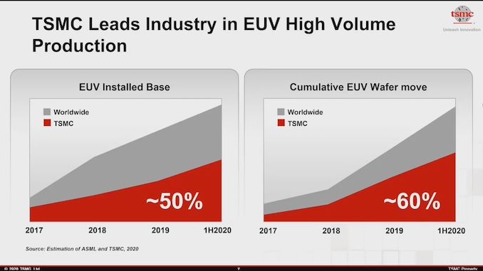
One of the overriding central messages to TSMC’s Technology Symposium this week is that the company is a world leader in semiconductor manufacturing, especially at the leading edge process technology. To further hit the message home, TSMC showcased a slide indicating where it stands in relation to others: by using a combination of public ASML statements and their own internal purchase sheets, TSMC predicts that they have ~50% of all the active EUV machines installed worldwide. Beyond that, the company also has a number of ~60% for cumulative EUV wafer production.
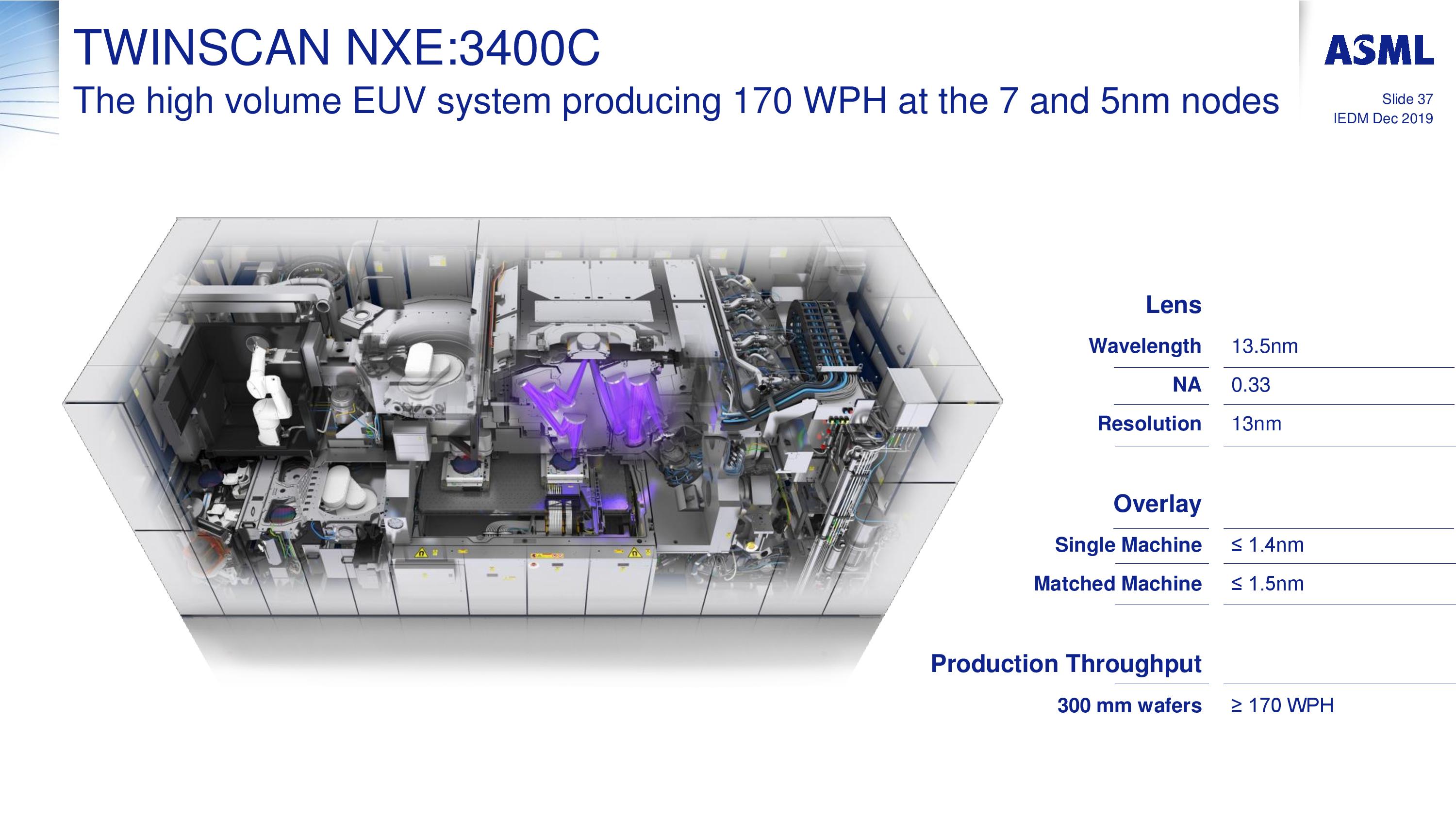
Current known public EUV processes from the big fabs include TSMC’s 7+ and N5, as well as Samsung’s 7LPP (and anything below), with Intel’s EUV efforts only entering in its own 7nm portfolio next year. Anything beyond these processes at the leading edge will continue to extend EUV use. EUV machines typically have a lower throughput, anywhere from 120-175 wafers per hour, than regular DUV machines which can reach 275 wph on the latest versions, however since 1 layer of EUV typically replaces 3-4 layers of DUV, the throughput is higher, but nonetheless the desire to scale out to multiple EUV machines to increase the physical number of wafers is a keen target for these foundries.
The only company that makes EUV machines is ASML, and the company publically announces how many machines it sells each year. The details are as follows:
| ASML's EUV Shipments | ||||||||||||||||||
| 2015 | 2016 | 2017 | 2018 | 2019 | 2020 | 2021 | ||||||||||||
| Actual | 2 | 4 | 10 | 3 | 4 | 5 | 6 | 4 | 7 | 7 | 8 | 4 | 9 | - | - | - | ||
| Target | - | - | - | 20 | 30 | 35 | 45-50 | |||||||||||
| 2018 and beyond is split per quarter for actual shipped numbers Data taken from ASML's Financial Reports |
||||||||||||||||||
Note that each year so far, ASML hasn’t quite hit its targets, but has done near enough, although sales in Q1 2020 were lower than I would expect, indicating that by end of Q2 2020, ASML has only shipped 13 out of the proposed 35 systems. These numbers include all the different types of Twinscan NXE machines that ASML has built, with the more recent ones having better throughput (and sometimes the older ones get retrofitted). As of the end of Q2 2020, we predict that ASML has shipped around 71 of these EUV machines, and will likely hit 90 by the end of 2020. Some observers have noted that ASML may have a backlog of as many as 49 EUV scanner orders, even with these shipment targets.

If ASML has shipped 71 machines, that would mean, according to TSMC’s numbers, the company has around 30-35. Note that TSMC’s numbers are for ‘Installed EUV’ machines – we learned from our trip to GlobalFoundries in Q1 2018 that it takes up to 6 months from getting the parts to calibrating the machine for use. At present, some of these foundries therefore have EUV machines sitting around waiting to be installed, or in the case of Intel, perhaps only in use for early testing or pre-risk trials. We know that GlobalFoundries had two early EUV machines, installed one, but ended up selling both when it decided not to pursue leading edge 7nm, and SMIC ordered one but as far as we know it wasn’t installed due to restrictions imposed by the US.
As TSMC grows its Fab 18 for N5 production, and ramps its EUV integration, it will be interesting to see if TSMC is ever limited by the number of machines it has. At some point Intel is going to want to buy a number when it deploys its 7nm processes (I’ve seen predictions that Intel has at least ~10 machines already, but I can’t confirm that) as well, so there might be a tussle for who gets their order delivered first.
One thing is for sure however, ASML is sitting pretty right in the middle with a monopoly on everything. I still have an invite to visit one of their EUV machine factories in Connecticut, which when the COVID mess is all over I intend to follow up on. It should be exciting.
Related Reading
- SMIC Details Its N+1 Process Technology: 7nm Performance in China
- GlobalFoundries Stops All 7nm Development: Opts To Focus on Specialized Processes
- Intel 7nm Delayed By 6 Months; Company to Take “Pragmatic” Approach in Using Third-Party Fabs
- TSMC: N7+ EUV Process Technology in High Volume, 6nm (N6) Coming Soon
- TSMC: 3nm EUV Development Progress Going Well, Early Customers Engaged
- TSMC’s 5nm EUV Making Progress: PDK, DRM, EDA Tools, 3rd Party IP Ready
- ASML’s First Multi-Beam Inspection Tool for 5nm
- TSMC Expects 5nm to be 11% of 2020 Wafer Production (sub 16nm)
- ‘Better Yield on 5nm than 7nm’: TSMC Update on Defect Rates for N5
- TSMC Details 3nm Process Technology: Full Node Scaling for 2H22 Volume Production
- TSMC Confirms Halt to Huawei Shipments In September


32 Comments
View All Comments
LAZRJOCK - Friday, August 28, 2020 - link
What comes after EUV you ask? molecular level. Asml has nothing in the pipe line for that. A higher N.A. isnt going to do the trick then.catavalon21 - Thursday, August 27, 2020 - link
A high P/E ratio?Yojimbo - Saturday, August 29, 2020 - link
High valuation is the only reason. You're a little late to the party. But that doesn't mean it isn't a good investment. Notice how the companies who design cutting-edge logic chips are stressing "it's the architecture that's important"? That's because it's getting more and more expensive to use the latest logic processes. They are sharing more and more of their revenue with the manufacturing services. And the manufacturing is capital intensive and takes a high degree of technical skill. So foundries and chip equipment makers will capture a greater percentage of the hardware pie. This is why it's important for chip companies to develop platforms to ensure profit margins. For a while now, server and PC makers have made hardly any profit, as all the profit goes to the makers of the chips that demand a lot of work to design, and because it's the chip makers that define the platform, not the server/PC makers. If that margin on chips gets siphoned off to foundries and chip equipment makers the chip makers will especially need vibrant platforms to maintain their margins, but the trend would be that chip equipment makers like ASML should benefit with secular growth and margin expansion.oak8292 - Thursday, August 27, 2020 - link
I have been curious about the availability of EUV equipment based on the reported back log of EUV machines. If AMD, Intel or somebody else wants additional N6 or N5 wafers can TSMC provide them. Here is the comment from the last ASML quarterly conference.'We are still planning at capacity of 45 to 50 systems next year. They just planned within our existing factory footprint by reducing cycle time in our factory to around 20 weeks by the end of this year, currently have a backlog of 54 systems with 28 system orders for 2021 delivery, covering over half of this capacity, and we expect orders to continue in the second half of the year in support of the 2021 demand.' (Sourced from SA Earnings Call Transcript.)
Based on the 28 machines scheduled for delivery in 2021 it looks like there are still 17-22 EUV machines that could be ordered for deliver in 2021. With a six month set up it could be 2022 before actual additional capacity is on line.
LAZRJOCK - Friday, August 28, 2020 - link
I worked for ASML for 9 years. install for another vendor now. installed and set up, integrated for customer. the wafer and reticle stages are under vacuum allowing them a cost saving by returning to the original interferometer om IMF. customer won't see that. Density wise intels 10 is better than tmsc's 7. I've been to fab 15. 18 wasn't built yet. I've been in Intel D1C,D,and X in building R4. Also fab42 which has capacity of 8 machines but only has 2. 8 are installed in Oregon D1X fab. EUV is all CO2 lasers. Trumph just pumps the signal through 5 separate amplifying cavities to acquire the need gain to reach 260W. But 4 watts at the wafer would burn at 10nm. so 4W using zernike indices they get the imaging down to mere Nanowatts actually being delivered to the photo resist. TSMC right now is smoke and mirrors. dont let the smaller figures fool you. Intel still has a much stronger architecture. With a consistent 99 percent yield TSMC still has some ground to make up.Spunjji - Friday, August 28, 2020 - link
Weird flexes at several points here:"Density wise intels 10 is better than tmsc's 7"
This is not borne out in practice for die size vs. transistor count on Ice Lake or Lakefield. Intel had a theoretical density advantage which they had to burn to get the process to yield. They're notably not talking density for 10++/SF.
"Intel still has a much stronger architecture. With a consistent 99 percent yield TSMC still has some ground to make up."
Eh? Intel's yields on 10nm are still dismal. 14nm yields are almost certainly better, but that's not much use when that process is significantly less dense.
Duncan Macdonald - Friday, August 28, 2020 - link
I wonder how long it will be before free electron lasers are able to replace the current tin plasma source. (Starting with a laser source should allow a reduction in the number of mirror stages and elimination of plasma damage.)LAZRJOCK - Friday, August 28, 2020 - link
the collectors in the projection optics box or the POB. thats in the immediate future. athe closer the wafer to the source the clearer the imaging and even closer overlay than 2nm Ioverlay is at now.
LAZRJOCK - Friday, August 28, 2020 - link
Plus they ate always looking at different coatings for the mirrors to help with that exact reason.Anymoore - Friday, August 28, 2020 - link
They've been running 1000-1500 wpd (at most ~60 wph effectively).