The NVIDIA GeForce GTX 1650 Review, Feat. Zotac: Fighting Brute Force With Power Efficiency
by Ryan Smith & Nate Oh on May 3, 2019 10:15 AM ESTTU117: Tiny Turing
Before we take a look at the Zotac card and our benchmark results, let’s take a moment to go over the heart of the GTX 1650: the TU117 GPU.
TU117 is for most practical purposes a smaller version of the TU116 GPU, retaining the same core Turing feature set, but with fewer resources all around. Altogether, coming from the TU116 NVIDIA has shaved off one-third of the CUDA cores, one-third of the memory channels, and one-third of the ROPs, leaving a GPU that’s smaller and easier to manufacture for this low-margin market.
Still, at 200mm2 in size and housing 4.7B transistors, TU117 is by no means a simple chip. In fact, it’s exactly the same die size as GP106 – the GPU at the heart of the GeForce GTX 1060 series – so that should give you an idea of how performance and transistor counts have (slowly) cascaded down to cheaper products over the last few years.
Overall, NVIDIA’s first outing with their new GPU is an interesting one. Looking at the specs of the GTX 1650 and how NVIDIA has opted to price the card, it’s clear that NVIDIA is holding back a bit. Normally the company launches two low-end cards at the same time – a card based on a fully-enabled GPU and a cut-down card – which they haven’t done this time. This means that NVIDiA is sitting on the option of rolling out a fully-enabled TU117 card in the future if they want to.
By the numbers, the actual CUDA core count differences between GTX 1650 and a theoretical fully-enabled GTX 1650 Ti are quite limited – to the point where I doubt a few more CUDA cores alone would be worth it – however NVIDIA also has another ace up its sleeve in the form of GDDR6 memory. If the conceptually similar GTX 1660 Ti is anything to go by, a fully-enabled TU117 card with a small bump in clockspeeds and 4GB of GDDR6 could probably pull far enough ahead of the vanilla GTX 1650 to justify a new card, perhaps at $179 or so to fill NVIDIA’s current product stack gap.
The bigger question is where performance would land, and if it would be fast enough to completely fend off the Radeon RX 570. Despite the improvements over the years, bandwidth limitations are a constant challenge for GPU designers, and NVIDIA’s low-end cards have been especially boxed in. Coming straight off of standard GDDR5, the bump to GDDR6 could very well put some pep into TU117’s step. But the price sensitivity of this market (and NVIDIA’s own margin goals) means that it may be a while until we see such a card; GDDR6 memory still fetches a price premium, and I expect that NVIDIA would like to see this come down first before rolling out a GDDR6-equipped TU117 card.
Turing’s Graphics Architecture Meets Volta’s Video Encoder
While TU117 is a pure Turing chip as far as its core graphics and compute architecture is concerned, NVIDIA’s official specification tables highlight an interesting and unexpected divergence in related features. As it turns out, TU117 has incorporated an older version of NVIDIA’s NVENC video encoder block than the other Turing cards. Rather than using the Turing block, it uses the video encoding block from Volta.
But just what does the Turing NVENC block offer that Volta’s does not? As it turns out, it’s just a single feature: HEVC B-frame support.
While it wasn’t previously called out by NVIDIA in any of their Turing documentation, the NVENC block that shipped with the other Turing cards added support for B(idirectional) Frames when doing HEVC encoding. B-frames, in a nutshell, are a type of advanced frame predication for modern video codecs. Notably, B-frames incorporate information about both the frame before them and the frame after them, allowing for greater space savings versus simpler uni-directional P-frames.
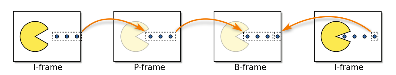
I, P, and B-Frames (Petteri Aimonen / PD)
This bidirectional nature is what make B-frames so complex, and this especially goes for video encoding. As a result, while NVIDIA has supported hardware HEVC encoding for a few generations now, it’s only with Turing that they added B-frame support for that codec. The net result is that relative to Volta (and Pascal), Turing’s NVENC block can achieve similar image quality with lower bitrates, or conversely, higher image quality at the same bitrate. This is where a lot of NVIDIA’s previously touted “25% bitrate savings” for Turing come from.
Past that, however, the Volta and Turing NVENC blocks are functionally identical. Both support the same resolutions and color depths, the same codecs, etc, so while TU117 misses out on some quality/bitrate optimizations, it isn’t completely left behind. Total encoder throughput is a bit less clear, though; NVIDIA’s overall NVENC throughput has slowly ratcheted up over the generations, in particular so that their GPUs can serve up an ever-larger number of streams when being used in datacenters.
Overall this is an odd difference to bake into a GPU when the other 4 members of the Turing family all use the newer encoder, and I did reach out to NVIDIA looking for an explanation for why they regressed on the video encoder block. The answer, as it turns out, came down to die size: NVIDIA’s engineers opted to use the older encoder to keep the size of the already decently-sized 200mm2 chip from growing even larger. Unfortunately NVIDIA isn’t saying just how much larger Turing’s NVENC block is, so it’s impossible to say just how much die space this move saved. However, that the difference is apparently enough to materially impact the die size of TU117 makes me suspect it’s bigger than we normally give it credit for.
In any case, the impact to GTX 1650 will depend on the use case. HTPC users should be fine as this is solely about encoding and not decoding, so the GTX 1650 is as good for that as any other Turing card. And even in the case of game streaming/broadcasting, this is (still) mostly H.264 for compatibility and licensing reasons. But if you fall into a niche area where you’re doing GPU-accelerated HEVC encoding on a consumer card, then this is a notable difference that may make the GTX 1650 less appealing than the TU116-powered GTX 1660.


126 Comments
View All Comments
onbquo - Friday, May 3, 2019 - link
Why is it nobody talking about coming 7nm Radeons mopping the floor in the 75W segment?PeachNCream - Friday, May 3, 2019 - link
Because no one has been able to benchmark said graphics cards so no one knows if something is going to mop floors or just draw polygons. (Personally, I'm in for a GPU that will mop my floors for me. I'd also like one that will mow the yard, wash the dishes, and take care of the laundry.)onbquo - Friday, May 3, 2019 - link
Good point but I seriously believe the next architecture Radeon built on 7nm could perform almost twice as fast than a RX 560 with 1024 CUs. Am I the only one hyped for 7nm graphics cards?guidryp - Friday, May 3, 2019 - link
You are making a pile of assumptions with no evidence.Process bumps aren't the big win that they once were. Radeon 7 is 7nm and it didn't get twice as fast. RTX2080 outperforms it while using less power.
7nm is NOT a magic bullet. We need to wait and see what actually happens.
Cooe - Friday, May 3, 2019 - link
More recent benchmarking actually shows the RVII with the performance edge vs the RTX 2080 (AMD just completely botched the launch drivers-wise, as isn't particularly uncommon for them) as many recent videos have shown, but you're totally passing over the fact that it uses the exact same Vega architecture as 14nm Vega 10 but manages to outperform it by around 30% while pulling LESS power than a V64. That's nearly a 40-50% boost in power efficiency per fps, with absolutely no arch changes beyond 2x additional memory controllers. Even if Navi only matches that kind of efficiency bump vs Polaris it'll still be looking really good just as long as they maintain their performance advantage as well.guidryp - Saturday, May 4, 2019 - link
Better in one or two AMD favorable games, but not overall. Beating power of V64 is needed, but still doesn't come close to NVidia power usage.Oxford Guy - Saturday, May 4, 2019 - link
7nm TSMC isn't nearly as impressive as 5nm TSMC. 80% increase in density with 5nm. 7nm is a little bit sad, really. But, it saves companies money because it doesn't require nearly as much design rules modification, so porting existing 14nm stuff is much easier.PeachNCream - Tuesday, May 7, 2019 - link
I'm really looking forward to seeing what 7nm GPUs do once they hit the market, but I want to hold back on making judgements before we see what sorts of performance and power numbers emerge. I'm also more interested in mobile than desktop components because I have not put together or purchased a desktop PC in the past 5 years since I find laptops and phones a better fit in my living space and lifestyle.nevcairiel - Saturday, May 4, 2019 - link
Personally, the only reason I would ever care about a 75W card is for video duties - and AMDs video decoding/encoding is significantly worse then Intels or NVIDIAs. So there is that.I would be excited if they were trying to make a high-end 7nm card that doesn't suck, but apparently its once again just low-power cards. same old same old. I'm bored already.
Oxford Guy - Saturday, May 4, 2019 - link
"Personally, the only reason I would ever care about a 75W card is for video duties "Then the lack of B frame support in the encoder is a deal-breaker.