GlobalFoundries Announces 22FDX Milestone: $2 Billion in Design Wins
by Anton Shilov on July 10, 2018 9:00 AM EST- Posted in
- Semiconductors
- GlobalFoundries
- FD-SOI
- 22FDX
GlobalFoundries on Monday announced a milestone concerning its 22FDX-branded fully-depleted SOI low-power planar transistor platform. The company initiated volume production using the technology with yields and performance meeting expectations of its clients. So far, the company has gained over 50 client designs and has booked contracts worth $2 billion.
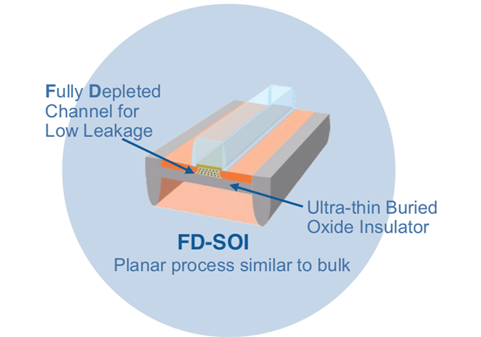
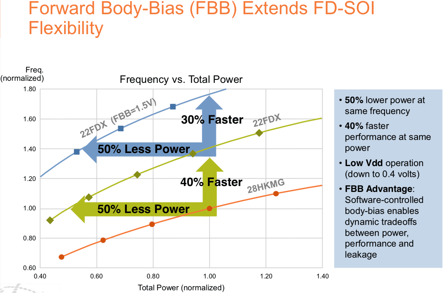
GlobalFoundries’ positions its 22FDX manufacturing technology as a cheaper alternative to 14 nm/16 nm FinFET fabrication processes. Since the 22FDX relies on planar transistors as well as fully-depleted SOI wafers, it is easier and cheaper to use than FinFET-based technologies. Another key feature of FD-SOI is very low static and dynamic power consumption, low voltages (down to 0.4 Volts) and software-controlled transistor body-biasing (up to 1.5V, which helps increase performance), all of which makes the process very appealing for mobile, wearables, IoT, RF and other applications. Since such chips are developed by startups without a lot of money, relatively low development costs are crucial for such companies.
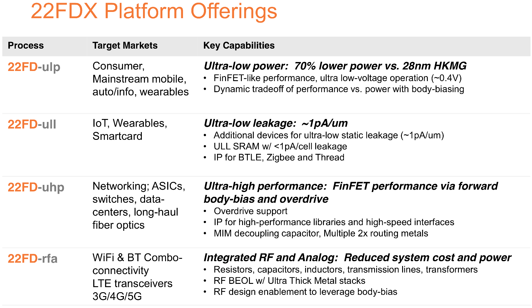
GlobalFoundries formally introduced its 22FDX platform — which includes four different manufacturing technologies for various applications — in mid-2015 and started early production this year. One of the first customers to use the GlobalFoundries’ 22FDX platform is Synaptics, but previously GlobalFoundries mentioned Cisco, Freescale and Sony as adopters of the technology.
According to GlobalFoundries, the 22FDX has booked customers’ orders worth $2 billion, which is a lot. To put this number into perspective, GlobalFoundries earned $6.176 billion in revenue last year. Meanwhile GlobalFoundries does not share any additional details about the 22FDX wafer revenue so we do not know the amount of time it will take GlobalFoundries to actually get these money.

Related Reading
- Change of Strategy: A New GlobalFoundries CEO in Dr. Thomas Caulfield
- GlobalFoundries Gives 7 nm Capacity Update, Mulls Skipping 5 nm
- The Future of Silicon: An Exclusive Interview with Dr. Gary Patton, CTO of GlobalFoundriess
- GlobalFoundries to Expand Capacities, Build a Fab in China
- GlobalFoundries Updates Roadmap: 7 nm in 2H 2018, EUV Sooner Than Later?
Source: GlobalFoundries


12 Comments
View All Comments
Death666Angel - Tuesday, July 10, 2018 - link
FinFET from GloFo is 14nm and 12nm, TSMC has 16nm. But these all mean little on their own. Current FinFET processes are geared for high performance. This is geared for low power consumption at adquate performance. Hence why a low power device functions better on the corresponding low power node. I wouldn't want a GPU or CPU made on this process, I doubt it would clock as well or as efficiently.wizfactor - Tuesday, July 10, 2018 - link
For some reason the first use-case that came to mind for me was the Raspberry Pi. I believe its SoC has been stuck at 40nm for a long time now, so I wonder if this would make a nice process for Broadcom if they choose to skip 28nm (assuming 22FDX isn't a bank breaker for this market segment).