Qualcomm Announces Snapdragon 845 Mobile Platform: Tocks Next-Gen CPU Cores, GPU, AI, & More
by Andrei Frumusanu on December 6, 2017 5:30 PM EST- Posted in
- Mobile
- Snapdragon
- Qualcomm
- Smartphones
- SoCs
- 10nm
- Snapdragon 845

Today as part of its media event, Qualcomm finally announced the much expected Snapdragon 845, successor to last year's very successful Snapdragon 835. The Snapdragon 845 is a large step in terms of SoC architectures as it's the first to employ ARM's DynamiQ CPU cluster organization. Quickly explained, DynamIQ enables the various different CPU cores within an SoC to be hosted within the same cluster and cache hierarchy, as opposed to having separate discrete clusters with no shared cache between them (with coherency instead happening over an interconnect such as ARM's CCI). This major transition is probably the largest to date that we've seen in modern mobile smartphone ARM consumer SoCs.
| Qualcomm Snapdragon Flagship SoCs 2017-2018 | |||
| SoC | Snapdragon 845 | Snapdragon 835 | |
| CPU | 4x Kryo 385 Gold (A75 derivative) @ 2.8GHz 4x256KB L2 4x Kryo 385 Silver (A55 derivative) @ 1.80GHz 4x128KB L2 2MB L3 |
4x Kryo 280 Gold (A73 derivative) @ 2.45GHz 2MB L2 4x Kryo 280 Silver (A53 derivative) @ 1.90GHz 1MB L2 |
|
| GPU | Adreno 630 | Adreno 540 @ 670/710MHz | |
| Memory | 4x 16-bit CH @ 1866MHz LPDDR4x 29.9GB/s 3MB system cache |
4x 16-bit CH @ 1866MHz LPDDR4x 29.9GB/s |
|
| ISP/Camera | Dual 14-bit Spectra 280 ISP 1x 32MP or 2x 16MP |
Dual 14-bit Spectra 180 ISP 1x 32MP or 2x 16MP |
|
| Encode/ Decode |
2160p60 10-bit H.265 720p480 |
2160p30 (2160p60 decode), 1080p120 H.264 & H.265 |
|
| Integrated Modem | Snapdragon X20 LTE (Category 18/13) DL = 1200Mbps 5x20MHz CA, 256-QAM UL = 150Mbps 2x20MHz CA, 64-QAM |
Snapdragon X16 LTE (Category 16/13) DL = 1000Mbps 3x20MHz CA, 256-QAM UL = 150Mbps 2x20MHz CA, 64-QAM |
|
| Mfc. Process | 10nm LPP | 10nm LPE | |
The CPU
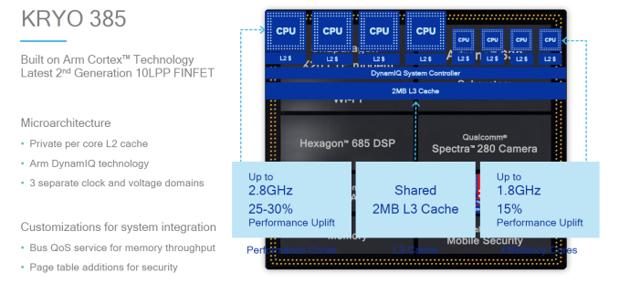
The Snapdragon 835's Kryo 280 performance and efficiency cores make use of ARM's Built on ARM Cortex Technology license which allows Qualcomm to make requests to ARM to change some aspects of the architectures of newly released cores and implement these changes exclusively into Snapdragon SoCs. As such the S835's CPU cores were derivatives of ARM's Cortex A73 and Cortex A53 CPU IPs. The Snapdragon 845 being the first SoC to be based on a DynamIQ big.LITTLE CPU organization also undoubtedly suggests that the Kryo 385 CPUs are based on ARM's Cortex A75 and Cortex A55 IPs, as these are the only DynamIQ compatible CPU cores available to date.
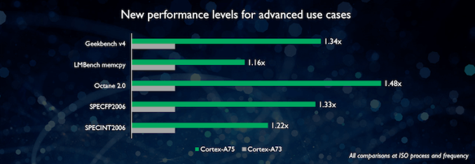
The Kryo 385 gold/performance cluster runs at up to 2.8GHz, which is a 14% frequency increase over the 2.45GHz of the Snapdragon 835's CPU core. But we also have to remember that given that the new CPU cores are likely based on A75's we should be expecting IPC gains of up to 22-34% based on use-cases, bringing the overall expected performance improvement to 39-52%. Qualcomm promises a 25-30% increase which is at the low-end of ARM's projections.
The silver/efficiency cluster is running at 1.8GHz, this is clocked slightly slower than the A53's on the Snapdragon 835 however the maximum clocks of the efficiency cluster is mainly determined by where the efficiency curve of the performance cluster intersects. Nevertheless the efficiency cores promise 15% boost in performance compared to its predecessor.
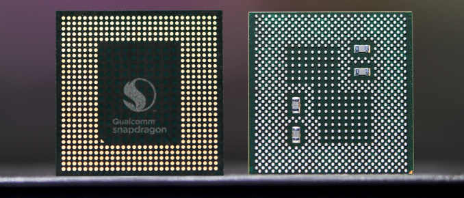
The new Snapdragon 845 now includes capacitors on its package underside
The L3 located on the DynamIQ DSU is configured at 2MB and we're likely seeing 256KB/128KB options for the performance and efficiency core private L2's. Together this would mean there's a total of 3.5MB of combined L2 and L3 cache on the CPU complex.
Qualcomm interestingly disclosed that we're only seeing three voltage and frequency planes implemented; likely meaning a single plane each for the performance cores as well as the efficiency cores as well as a plane for the L3 and DSU. This is surprising as DynamIQ allows finer grained frequency/voltage planes and given Qualcomm being traditionally a big proponent of asymmetric planes such as implemented in Krait I would have expected to see a more non-traditional approach, something that would have been facilitated given the fact that Qualcomm likes to include on-chip LDO regulators for powering the CPU clusters.
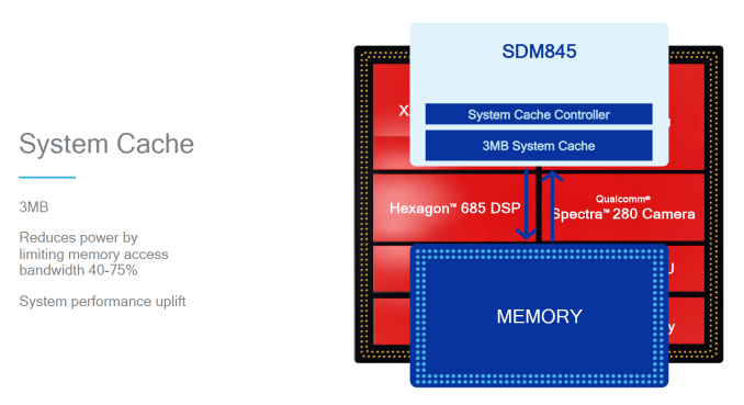
Related to the caches but not part of the CPU, there's also a new inclusion of a 3MB system cache. This is likely a SoC interconnect cache and serves all SoC blocks - likely in similar fashion the "L3" cache on Apple A-series SoCs works. This would help reduce external memory transactions and thus also reduce power to the memory controllers and DRAM. Qualcomm claims it's able to reduce memory access bandwidth by up to 40-75%, a significant figure.
The GPU
The Snapdragon 845 comes with a new generation of the Adreno GPU, called the Adreno 630. The switch from a 5xx family to a 6xx family GPU, as with previous introductions from Qualcomm usually marks the transition consisting of larger architectural changes.
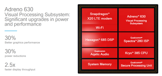
Qualcomm is as usual very tight-lipped about details of its GPU but it promises a performance increase of 30% while also increasing power-efficiency by 30%. What this translates to is basically we're looking at 30% higher frame-rates while maintaining the same power consumption of the Snapdragon 835, which is an excellent improvement.
DSP Upgrade to Hexagon 685
The DSP sees a evolutionary upgrade from the 682 to the 685. Again details about the improvements are relatively sparse but Qualcomm promises improvements in power and performance, especially for AI and imaging tasks. Qualcomm made an emphasis on AI processing during the presentation and claim that the new IP achieves up to 3x increase in performance compared to the Snapdragon 835.
Traditional DSP architectures are usually not well optimized for neural network processing so we'll have to adopt a wait & see approach when it comes to the performance of the new Hexagon 685 when executing such tasks. SoCs which have a dedicated NPU such as the Apple A11 or Kirin 970 still have a large edge here as they augment the image processing pipeline instead of handing such tasks over to the DSP which might have to do double duty of both image processing (such as HDR) and image analysis via neural network processing (image recognition and classification).
Snapdragon X20 Modem Now Integrated
As is traditional with Qualcomm we first see cutting-edge modem implementations first released as independent discrete modems and only afterwards do we see them integrated into the newest high-end SoCs. The Snapdragon 845 now integrated the X20 modem released earlier in the year which we've covered in a dedicated article.
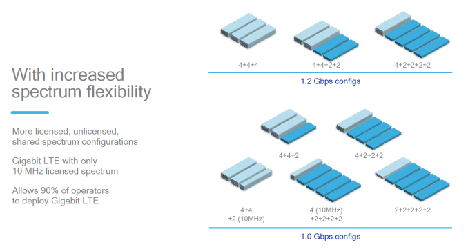
The new modem elevates the LTE UE Category to 18 as it's now capable of 5xCA as opposed to 4xCA on the X16 modem integrated in the Snapdragon 835. This allows for download speeds of up to 1.2Gbps when in a 5x20MHz downstream carrier aggregation mode, that is of course, if you're lucky enough for your mobile carrier to support such configurations.
Improved Media Capabilities
The Snapdragon 845's display pipeline receives an upgrade for VR and claims to be now able to drive dual-2400x2400p120 displays for VR headsets. The video recording capabilities have been improved as the Snapdragon 845 increases maximum video encoding framerate at 4K recording from 30 to 60fps compared to the Snapdragon 835. Qualcomm advertised support for Rec.2020 wide gamut color space recording, meaning we now see full support for HDR10 HEVC recording which should be an interesting addition I'm looking forward to test.
The new Spectra 280 ISP's most standout feature seems to be multi frame noise reduction (MFNR) which is a feature that I believe is also used in Google's HDR+ proprietary processing. The feature captures multiple pictures in fast succession and applies an algorithm to apply noise reduction in higher quality fashion compared to traditional single-frame noise reduction which can introduce blurriness.
Manufactured on Second Generation 10LPP Process
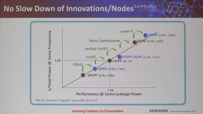
The Snapdragon 845 comes manufactured on a second generation 10LPP process from Samsung. This was a natural evolution to be expected as the Snapdragon 835 was manufactured on 10LPE. Samsung promises performance increase of up to 10% at the same power levels or reduced power consumption of up to 15% at the same performance. Samsung had just announced last week the start of mass production for 10LPP. I was rather surprised to see the larger frequency boost to 2.8GHz on the performance cores as the Snapdragon 835 came with rather conservative frequencies of only 2.45. The A75 promised increased performance at the same efficiency, meaning the core uses more power to reach the higher performance point compared to the A73.
Most devices I've seen with Snapdragon 835's used about 1.1W per core at peak using the power virus-style workload we traditionally use so seeing the Snapdragon 845 using the new processor architecture as well as increases in frequency is quite surprising as both would increase the absolute power consumption of the CPUs. The two possible scenarios we're likely to encounter is that either the Snapdragon 845 CPU complex uses more power or that Samsung has managed to vastly improve its manufacturing process over the last year to allow for such gains.
"Tock" Generation For CPU and GPU
The new Snapdragon 845 brings with itself one of the biggest architectural shifts in the ARM SoC space with the first implementation of the new DynamIQ cluster hierarchy. With an expected solid 30% performance boost on both CPU and GPU we're likely to see a healthy upgrade for 2018 flagship devices. Overall the Snapdragon 845 fulfils most of its expectations and in a time in the Android ecosystem where improvements have slowed down this is a good thing. The Snapdragon 835 was an excellent SoC as it balanced performance and power perfectly and thus re-solidified Qualcomm's positioning as the go-to solution for mobile SoCs. On paper the Snapdragon 845 seems to continue this balance and if all goes as planned we're likely to see another healthy generation of devices in 2018 that we're eagerly awaiting to review.




145 Comments
View All Comments
Andrei Frumusanu - Saturday, December 9, 2017 - link
GeekBench changed the memory latency subtest in GB 4.1 and it gives a lower score than GB 4.0. All ~2100ish numbers are GB 4.0.Wilco1 - Saturday, December 9, 2017 - link
That may cause some of the difference, but not nearly all. Consider eg. https://browser.geekbench.com/v4/cpu/compare/52738...If you ignore the memory score, the crypto/int/fp results for the S8 are exactly what you'd expect when running between 2.25 and 2.35GHz. The AES test shows the actual frequency the CPU runs at.
peevee - Thursday, December 7, 2017 - link
Where do you see the test result?MonkeyPaw - Wednesday, December 6, 2017 - link
Yeah, the scale of the graphs are definitely misleading. If something isn't even 2x the performance baseline, then the bar shouldn't blow well past the 2x mark. That's not to take away from the actual performance gains, but it's definitely on the misleading side.Frenetic Pony - Wednesday, December 6, 2017 - link
Can the DSP also be configured for AV1? The standard should (theoretically) be locked down this year. And Google refuses to pay the HEVC payments for Android, as do (apparently) everyone but the richest handset sellers. Meaning AV1 will, in all likelihood, be the HDR choice for both video and stills next year.Andrei Frumusanu - Wednesday, December 6, 2017 - link
Video encoding happens on the Venus fixed function blocks so it's unlikely it'll ever get any other codec support.mode_13h - Wednesday, December 6, 2017 - link
Hopefully this will make 835-based devices more affordable. I'm not about to spend close to $1k on a smartphone.Also, I thought we'd be seeing HBM2 in mobile, by now. I guess it's probably still too expensive.
extide - Thursday, December 7, 2017 - link
Doubt we will see HBM in mobile ever. It's way overkill, takes up too much board space, too much power, etc.mode_13h - Saturday, December 9, 2017 - link
HBM2 is *more* power-efficient and denser than DDR4. This is exactly why it's only a matter of time.MrSpadge - Thursday, December 7, 2017 - link
They don't even generally use 128 bit DDR4, so even a single HBM stack would be total overkill.